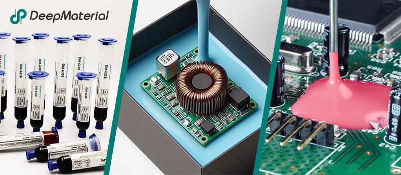
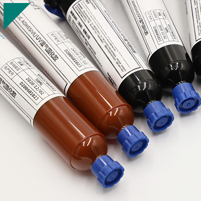
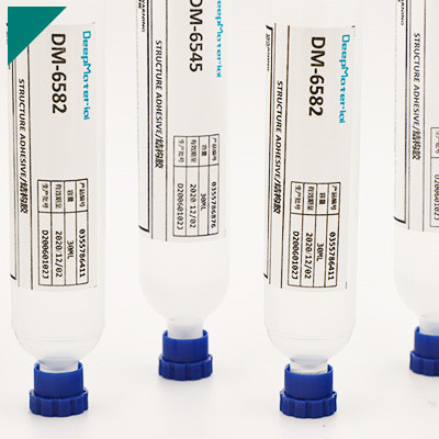
Home > Potting Compound > UV Cure Potting Compound
UV Cure Potting Compound
In the realm of electronics protection, UV cure potting compound stands as a beacon of innovation, offering a myriad of benefits that revolutionize traditional potting methods. Harnessing the power of ultraviolet light, these compounds provide rapid curing, exceptional strength, and versatility in application. Join us on a journey to unravel the mysteries behind UV cure potting compound and discover its extraordinary potential in safeguarding electronic components.
Table of Contents
ToggleWhat Makes UV Cure Potting Compound Different from Traditional Potting Compounds?
UV cure potting compounds, which differ from conventional potting compounds in several ways, have completely changed the electronics encapsulating industry. Because of their special qualities and advantages, these contemporary solutions are becoming increasingly well-liked across a range of industries.
Traditional potting compounds typically rely on heat or chemical reactions to cure, often resulting in longer processing times and limited control over the encapsulation process. In contrast, UV cure potting compounds rapidly solidify when exposed to ultraviolet light, significantly reducing curing times and allowing for greater precision in manufacturing processes. The accelerated curing process improves production efficiency and enhances overall product quality.
One key advantage of UV cure potting compounds is their ability to provide precise control over the encapsulation process. Manufacturers can adjust parameters such as UV light intensity and exposure time to achieve uniform encapsulation of electronic components, ensuring consistent quality and performance in the finished product. This level of control is precious in industries where reliability and precision are critical, such as aerospace and medical devices.
In addition to rapid curing and precise control, UV cure potting compounds offer enhanced performance compared to traditional alternatives. These compounds typically exhibit superior adhesion properties, forming strong bonds with various substrates, including metals, plastics, and ceramics. As a result, electronic devices encapsulated with UV cure compounds are better protected against moisture, chemicals, and mechanical stress, leading to increased reliability and longevity.
In addition, compared to solvent-based or heat-cured alternatives, UV cure potting ingredients are designed with fewer volatile organic compounds (VOCs) and dangerous chemicals. It makes them safer for workers and the environment and aligns with sustainability initiatives in manufacturing operations. Additionally, the energy-efficient curing process of UV cure compounds helps reduce overall energy consumption, further contributing to environmental preservation.
Another notable advantage of UV cure potting compounds is their versatility and adaptability to various application requirements. Whether encapsulating sensitive electronic components in consumer electronics or ruggedized systems in industrial machinery, UV cure compounds offer flexibility in design and application. Their compatibility with automated dispensing equipment makes them ideal for high-volume production, streamlining manufacturing processes and reducing costs.
How Does UV Cure Potting Compound Ensure Rapid Curing?
UV cure potting compound is a cutting-edge solution revolutionizing how electronic components are encapsulated and protected. By harnessing the power of ultraviolet light, this innovative material offers rapid curing times and unparalleled performance. Let’s delve into how UV cure potting compound achieves such efficiency:
Ultraviolet Activation:
- UV cure potting compounds contain photoinitiators that react when exposed to UV light.
- These photoinitiators trigger a polymerization reaction upon exposure, transforming the liquid compound into a solid material.
Instant Curing:
- Unlike traditional potting compounds that rely on heat or chemical reactions for curing, UV cure compounds solidify almost instantly upon exposure to UV light.
- This instantaneous curing process significantly reduces production time and increases efficiency.
Precise Control:
- UV cure potting compounds offer precise control over the curing process.
- Manufacturers can adjust light intensity, exposure time, and wavelength to tailor the curing process to specific applications.
Enhanced Productivity:
- Rapid curing times translate to enhanced productivity on the production line.
- Manufacturers can achieve higher throughput without compromising quality, leading to cost savings and increased competitiveness.
Superior Performance:
- UV cure potting compounds deliver excellent adhesion and encapsulation properties.
- The cured material forms a durable, protective barrier around electronic components, safeguarding them against moisture, chemicals, and mechanical stress.
Versatility:
- UV cure potting compounds are versatile and can be used in various industries.
- These compounds offer reliable protection in diverse environments, from automotive electronics to medical devices.
Environmental Benefits:
- UV cure technology is more environmentally friendly than traditional curing methods that may involve heat or solvent-based chemicals.
- It eliminates the need for volatile organic compounds (VOCs) and reduces energy consumption, contributing to sustainability efforts.
Consistent Results:
- UV cure potting compounds ensure consistent curing results batch after batch.
- Manufacturers can achieve uniform encapsulation and reliable product performance with proper process control and UV exposure parameters.
Can UV Cure Potting Compound Bond Effectively with Various Substrates?
UV cure potting compounds have gained significant popularity in various industries for their efficient curing process and excellent bonding properties. These compounds offer numerous advantages over traditional potting methods, making them a preferred choice for many applications. But can UV cure potting compounds effectively bond with various substrates? Let’s delve into this question.
Bonding with Different Substrates:
- Plastics: UV cured potting compounds stick to a wide range of plastics, including polycarbonate, ABS, and polyethylene, with remarkable ease. They bind firmly without causing any harm to the substrate.
- Metals: Whether aluminum, stainless steel, or copper, UV cure potting compounds adhere well to metal surfaces, providing reliable encapsulation for electronic assemblies in harsh environments.
- Glass: UV cure compounds can effectively bond with glass substrates, offering enhanced protection for sensitive electronic components in optical devices and sensors.
- Ceramics:Due to their versatility, UV cure potting compounds also bond effectively with ceramic materials, ensuring robust encapsulation for ceramic-based electronics.
- Composites:From fiberglass to carbon fiber, UV cure potting compounds provide strong adhesion to composite materials, making them suitable for encapsulating composite-based electronic assemblies in aerospace and automotive applications.
Advantages of UV Cure Potting Compounds:
- Rapid curing: UV cure compounds cure within seconds to minutes, significantly reducing production time.
- Precise application: These compounds can be applied precisely, minimizing waste and ensuring uniform encapsulation.
- Environmental friendliness: UV cured potting compounds typically contain fewer volatile organic compounds (VOCs) than conventional potting materials, contributing to a cleaner production process.
- Enhanced performance: Long-term dependability is ensured by UV cure materials’ exceptional mechanical strength, thermal stability, and resistance to environmental influences.
What Are the Environmental Benefits of UV Cure Potting Compound?
UV cure potting compound, known as UV curing resin, has gained significant traction in various industries due to its efficiency, versatility, and eco-friendly properties. This innovative material offers several environmental benefits, making it a preferred choice for manufacturers striving for sustainability. Let’s delve into the ecological advantages of UV cure potting compound:
Reduced Energy Consumption:
- UV cure potting compounds cure rapidly under ultraviolet light exposure, eliminating the need for prolonged heating.
- Traditional potting compounds often require significant energy consumption for curing through thermal methods, contributing to higher carbon emissions.
Lower Emissions:
- Unlike thermal curing processes that release volatile organic compounds (VOCs) into the atmosphere, UV cure potting compounds produce minimal to no emissions.
- Reducing emissions helps mitigate air pollution and promotes healthier indoor air quality.
Waste Reduction:
- UV cure potting compounds are formulated to cure precisely, minimizing material waste during manufacturing.
- Traditional potting compounds may involve excess material usage and scrap generation, leading to higher waste volumes in production.
Improved Worker Safety:
- UV cure potting compounds eliminate the need to handle hazardous chemicals typically found in traditional potting compounds.
- UV cure technology enhances workplace safety and health by removing exposure to toxic substances and reducing the risk of accidents.
Enhanced Product Durability:
- UV cure potting compounds offer superior adhesion and resilience, resulting in durable end products with extended lifespans.
- Enhanced durability reduces the frequency of repairs and replacements, contributing to resource conservation and waste reduction.
Energy Efficiency in End Use:
- Products encapsulated with UV cure potting compounds often exhibit superior thermal conductivity, enhancing energy efficiency during operation.
- Improved thermal management can reduce energy consumption in various applications, such as electronics and automotive components.
Are UV Cure Potting Compounds Resistant to Chemicals and Solvents?
UV cure potting compounds are polymers that solidify when exposed to ultraviolet (UV) light. This curing process occurs rapidly, making them ideal for applications with a quick production turnaround. These substances are highly valued because of their strong resistance to environmental elements like moisture, dust, and mechanical strain.
Chemical Resistance: A Critical Factor
One primary consideration when selecting potting compounds is their resistance to chemicals and solvents. Industries such as automotive, aerospace, and electronics rely on components that can withstand exposure to various chemical agents without compromising performance or integrity.
Assessing Chemical Resistance
UV cure potting compounds boast impressive chemical resistance and can withstand various solvents and chemicals commonly encountered in industrial environments. These compounds form a durable barrier that shields sensitive electronics from corrosive substances, ensuring prolonged reliability and functionality.
Factors Influencing Chemical Resistance
Several factors influence the chemical resistance of UV cure potting compounds:
- Chemical Composition:The potting compound’s chemical resistance largely depends on its formulation. Manufacturers often tailor formulations to enhance specific properties, including chemical resistance.
- Cross-Linking Density:Higher cross-linking density within the polymer matrix typically improves chemical resistance. This denser structure creates a more formidable barrier against solvent penetration.
- Curing Conditions: Proper curing under optimal conditions is imperative for achieving maximum chemical resistance. Adequate exposure to UV light ensures thorough polymerization, enhancing the compound’s overall durability.
Applications and Benefits
The chemical resistance of UV cure potting compounds makes them well-suited for a myriad of applications, including:
- Electronics: Protecting sensitive electronic components from exposure to moisture and corrosive chemicals.
- Automotive:To withstand harsh operating conditions, automotive systems’ sensors, connectors, and control units are encapsulated.
- Medical Devices:Ensuring the integrity of medical electronics subjected to sterilization processes and chemical disinfectants.
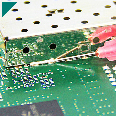
How Does UV Cure Potting Compound Enhance Thermal Management in Electronics?
UV cure potting compound is a specialized material used to encapsulate electronic components. It comprises polymers that solidify when exposed to ultraviolet (UV) light, forming a durable protective barrier around sensitive electronics.
Superior Thermal Conductivity:
One of the primary advantages of UV cure potting compound is its exceptional thermal conductivity. By efficiently dissipating heat away from electronic components, it prevents overheating and ensures stable operation even in demanding environments.
Enhanced Heat Dissipation:
Traditional potting compounds may impede heat dissipation due to their insulating properties. In contrast, the UV cured potting compound facilitates heat transfer, allowing for more effective cooling of electronic devices. This characteristic is especially crucial in high-performance applications where heat buildup can compromise functionality.
Precision Application:
UV cure potting compound offers precision application, enabling manufacturers to encapsulate intricate electronic assemblies easily. Its low viscosity allows it to flow into tight spaces, ensuring uniform coverage and eliminating air pockets that could impede thermal conductivity.
Rapid Cure Time:
Another significant advantage of the UV cure potting compound is its rapid cure time. Upon exposure to UV light, the compound cures within seconds, significantly reducing production time compared to traditional curing methods. This quick turnaround enhances manufacturing efficiency without compromising on quality.
Excellent Chemical Resistance:
In addition to its thermal properties, UV cure potting compound exhibits excellent chemical resistance, safeguarding electronics from moisture, corrosion, and other environmental factors. This durability ensures long-term reliability, even in harsh operating conditions.
Versatile Applications:
Numerous industries, including consumer electronics, telecommunications, automotive, and aerospace, use UV cure potting compounds. Its ability to enhance thermal management makes it indispensable in devices ranging from power converters and LED lighting to sensors and control modules.
Can UV Cure Potting Compound Facilitate Miniaturization of Electronic Devices?
UV cure potting compound is a specialized material used in electronic manufacturing processes. It is a type of resin that rapidly cures when exposed to ultraviolet (UV) light. This curing process transforms the liquid resin into a solid, providing protection and insulation to delicate electronic components.
- Enhanced Precision and Control : One of the primary advantages of UV cured potting compound is its ability to offer enhanced precision and control during manufacturing. Unlike traditional potting compounds that require time-consuming curing processes, UV cured compounds cure almost instantly when exposed to UV light. This rapid curing enables manufacturers to achieve greater precision in the encapsulation of electronic components, even in highly intricate designs.
- Reduced Footprint : Miniaturization often hinges on reducing the footprint of electronic components. UV cure potting compound enables manufacturers to achieve this goal by providing a thin yet durable layer of protection around sensitive components. This thin layer not only ensures robust insulation but also minimizes the device’s overall size, allowing for greater compactness without compromising functionality.
- Improved Thermal Management : Effective thermal management is crucial for the reliable operation of electronic devices, especially in compact designs where heat dissipation can be challenging. UV cure potting compounds offer excellent thermal conductivity, efficiently transferring heat away from critical components. By facilitating superior thermal management, these compounds contribute to the longevity and reliability of miniaturized electronic devices.
- Resistance to Environmental Factors : Electronic devices often face harsh operating environments, including exposure to moisture, chemicals, and temperature fluctuations. UV cure potting compounds provide a protective barrier that shields components from these environmental factors, enhancing their durability and reliability in challenging conditions.
- Streamlined Manufacturing Processes : The rapid curing properties of UV cure potting compounds streamline the manufacturing process, reducing production time and costs. With shorter curing times, manufacturers can achieve higher throughput and increased efficiency on the production line, ultimately accelerating time-to-market for miniaturized electronic devices.
What Role Does UV Cure Potting Compound Play in Improving Electrical Insulation?
Electrical insulation is a critical aspect of many electronic devices, ensuring safety, reliability, and longevity of operation. UV cure potting compound emerges as a key player in enhancing electrical insulation, offering a range of benefits for various applications. Let’s delve into the significance of UV cure potting compound in improving electrical insulation:
Enhanced Dielectric Properties:
- UV cure potting compounds possess excellent dielectric properties, effectively insulating electrical components.
- They provide high resistivity, minimizing the risk of electrical leakage and breakdown even under challenging conditions.
Rapid Cure Time:
- UV cure potting compounds cure rapidly upon exposure to ultraviolet light.
- This quick curing process reduces production time, enhancing overall efficiency and productivity in manufacturing processes.
Superior Adhesion:
- These compounds adhere strongly to various substrates, including metals, plastics, and ceramics, ensuring robust encapsulation of electronic components.
- Strong adhesion prevents moisture ingress and protects sensitive components from environmental factors, improving long-term reliability.
Thin Profile:
- UV cure potting compounds can be applied in thin layers while maintaining excellent insulation properties.
- This functionality benefits applications where weight or space restrictions are essential factors.
Chemical Resistance:
- UV cure potting compounds resist various chemicals, including solvents, oils, and harsh environmental elements.
- This resistance ensures prolonged protection for electronic components, even in demanding operating conditions.
Temperature Stability:
- These compounds offer remarkable thermal stability, maintaining their insulation properties over a wide temperature range.
- They can withstand elevated temperatures without compromising electrical performance, making them suitable for diverse applications.
Versatility:
- UV cure potting compounds are versatile and can be tailored to meet specific application requirements.
- They are available in various formulations, accommodating different curing mechanisms, viscosities, and thermal properties.
Are UV Cure Potting Compounds Compatible with High-Frequency Applications?
High-frequency applications encompass various electronic devices and systems, from radio frequencies (RF) to microwaves. These applications are prevalent in telecommunications, aerospace, medical devices, and various industrial sectors where signal integrity and performance are critical.
Advantages of UV Cure Potting Compounds
UV cure potting compounds offer several advantages that make them appealing for high-frequency applications. Their rapid curing properties allow for quick encapsulation of sensitive components, minimizing the risk of signal degradation due to prolonged exposure to environmental factors. Additionally, UV cure compounds provide excellent dielectric properties, ensuring efficient insulation and minimal interference with high-frequency signals.
Challenges in Compatibility
While UV cure potting compounds offer numerous benefits, compatibility with high-frequency applications can pose challenges. Traditional formulations may exhibit characteristics detrimental to signal integrity, such as excessive dielectric loss or poor thermal conductivity. Moreover, the curing process may introduce inconsistencies affecting high-frequency circuit performance.
Dielectric Properties and Signal Integrity
The dielectric properties of UV cure potting compounds play a crucial role in their compatibility with high-frequency applications. Low dielectric constant and dissipation factor are preferred characteristics to minimize signal loss and maintain signal integrity. Manufacturers must carefully select or customize UV cure compounds to meet the specific dielectric requirements of high-frequency circuits.
Thermal Management Considerations
Sustaining high-frequency circuit performance and dependability requires efficient thermal management. UV cure potting compounds with enhanced thermal conductivity can help dissipate heat efficiently, preventing overheating and signal degradation. Advanced formulations incorporating thermally conductive fillers or additives address the thermal challenges associated with high-frequency applications.
Testing and Validation
Ensuring the compatibility of UV cure potting compounds with high-frequency applications requires rigorous testing and validation procedures. Characterization of dielectric properties, signal integrity analysis, and thermal performance testing are essential in evaluating UV cure compounds’ suitability for specific high-frequency circuits.
How Does UV Cure Potting Compound Impact Production Efficiency?
UV cure potting compound, a key innovation in manufacturing, has revolutionized various industries by significantly enhancing production efficiency. This compound offers numerous benefits, making it a preferred choice for many applications. Let’s delve into how UV cure potting compound impacts production efficiency:
Rapid Curing Time:
- UV cure potting compounds cure almost instantly when exposed to ultraviolet light, leading to swift production cycles.
- Unlike traditional potting compounds, which require hours to cure, UV cure compounds streamline manufacturing processes by reducing curing time to mere seconds or minutes.
Increased Throughput:
- The quick curing nature of UV cure potting compounds enables manufacturers to increase throughput by minimizing downtime associated with curing processes.
- It accelerated curing time and increased production volumes within the same timeframe, enhancing overall productivity.
Precision and Consistency:
- UV cure potting compounds offer precise control over curing, ensuring consistent results across batches.
- Manufacturers can achieve uniform encapsulation and bonding, minimizing rework and rejection, thus optimizing production efficiency.
Energy Efficiency:
- UV curing requires minimal energy compared to thermal curing methods, contributing to reduced operational costs and environmental impact.
- Lower energy consumption translates to higher efficiency and cost savings in the long run, making UV cure potting compounds economically viable.
Versatility and Adaptability:
- UV cure potting compounds cater to diverse applications across industries such as electronics, automotive, aerospace, and medical devices.
- Their compatibility with various substrates and components allows for versatile use, simplifying production processes and inventory management.
Improved Quality Assurance:
The rapid curing and precise application of UV cure potting compounds minimize the risk of defects and ensure superior product quality.
- Enhanced quality assurance reduces the need for post-production inspections and rework, further streamlining manufacturing operations.
Enhanced Worker Safety:
- UV cure potting compounds eliminate the need for heat or solvent-based curing methods, reducing exposure to hazardous chemicals and fumes.
- Safer working conditions contribute to a healthier and more productive workforce, fostering a conducive manufacturing environment.
Can UV Cure Potting Compounds Be Applied in Harsh Environments?
UV cure potting compounds offer a fast and efficient solution for encapsulating electronic components, protecting against environmental factors while boasting rapid curing times. However, the question arises whether UV cure potting compounds can withstand the rigors of harsh environments. Exploring this query involves understanding the capabilities and limitations of UV-curable formulations in extreme conditions. Here’s an examination of whether UV cure potting compounds can be effectively applied in harsh environments:
- UV Resistance:UV cure potting compounds are formulated to cure first when exposed to ultraviolet (UV) light. While they exhibit excellent resistance to UV radiation during curing, prolonged exposure to UV light in harsh outdoor environments may cause degradation over time, reducing mechanical and optical properties.
- Temperature Extremes:Harsh environments often entail temperature extremes, including high heat or extreme cold. UV cure potting compounds may demonstrate varying degrees of thermal stability depending on their formulation. While some formulations can withstand elevated temperatures, others may become brittle or lose adhesion properties when exposed to extreme heat or cold.
- Chemical Exposure:Harsh environments may expose electronic devices to corrosive chemicals, solvents, or harsh cleaning agents. UV cure potting compounds may resist certain chemicals, but their compatibility varies depending on the formulation. Compatibility testing ensures the potting compound can withstand exposure to chemicals commonly encountered in harsh environments.
- Moisture and Humidity:Moisture ingress can significantly threaten electronic components, particularly in harsh outdoor or industrial environments. UV cure potting compounds may offer excellent moisture resistance when adequately cured, but prolonged exposure to high humidity levels or immersion in water may compromise their integrity over time.
- Mechanical Shock and Vibration:Electronic devices operating in harsh environments often encounter mechanical shock and vibration, which can compromise the integrity of the encapsulation. UV cure potting compounds should exhibit sufficient flexibility and impact resistance to withstand mechanical stresses without cracking or delaminating.
- Testing and Validation:UV cure potting compounds should undergo thorough testing and validation before deployment in harsh environments to assess their performance under simulated conditions. Testing methodologies may include accelerated aging tests, thermal cycling, humidity testing, and exposure to UV radiation to evaluate durability and reliability.
- Application Considerations:Proper application techniques are crucial for maximizing the performance of UV cure potting compounds in harsh environments. Adequate surface preparation, uniform application, and thorough curing are essential to ensure the integrity of the encapsulation and enhance resistance to environmental stresses.
What Quality Control Measures Are Implemented in UV Cure Potting Compound Manufacturing?
Stringent quality control measures are essential in the manufacturing process of UV cure potting compounds to guarantee that the finished product fulfills the requirements for performance and reliability. Various quality checks and controls are implemented from raw material selection to the final curing stage to guarantee consistency and efficacy. This article explores the critical quality control measures employed in UV cure potting compound manufacturing.
1. Raw Material Quality Control
- Selection Process:Thorough evaluation and testing of raw materials such as resins, additives, and photoinitiators to ensure they meet specified criteria.
- Supplier Assessment: Regular audits and assessments of suppliers to maintain quality consistency and reliability of sourced materials.
- Material Testing:Comprehensive testing for properties like viscosity, purity, and compatibility to ascertain suitability for the intended application.
2. Process Control
- Standard Operating Procedures (SOPs):Clear and detailed SOPs outlining each manufacturing process step to maintain consistency and repeatability.
- In-process Monitoring:Continuous monitoring of critical parameters like temperature, viscosity, and mixing ratios throughout production.
- Equipment Calibration: Regular calibration and maintenance to ensure accurate measurements and optimal performance.
3. Quality Assurance Testing
- Physical Properties Testing:Assessment of properties such as hardness, adhesion, and flexibility through standardized testing methods.
- Chemical Analysis:Analyze the chemical composition and curing kinetics to verify product integrity and performance.
- Accelerated Aging Tests:Environmental conditions are simulated to assess the durability and long-term stability of the cured compounds.
4. Final Product Inspection
- Visual Inspection:Examine the final cured product’s defects, such as air bubbles, cracks, or uneven curing.
- Dimensional Checks:Measurements of dimensions and thickness are conducted to ensure conformity to specifications.
- Performance Testing:Testing electrical, thermal, and mechanical properties to validate performance under various operating conditions.
Putting strict quality control procedures in place throughout the manufacturing process of UV cure potting compounds is vital to achieve consistent quality, reliability, and performance in the final product. By adhering to stringent standards and conducting careful examinations and testing, producers can guarantee that their UV cure potting compounds meet the demands of diverse applications in industries ranging from electronics to automotive and beyond.
Are UV Cure Potting Compounds Suitable for Outdoor Electronics?
Selecting a suitable potting compound is critical in electronics, mainly outdoor applications. Among the myriad options available, UV cure potting compounds have emerged as a promising choice due to their rapid curing process and excellent adhesion properties. However, the question persists: are UV cure potting compounds suitable for outdoor electronics? This exploration delves into the characteristics, advantages, challenges, and suitability of UV cure potting compounds in outdoor electronic applications.
Characteristics of UV Cure Potting Compounds:
UV cure potting compounds, renowned for their quick curing time, offer significant advantages over traditional potting materials. These compounds, comprising monomers and oligomers, remain liquid until exposed to ultraviolet (UV) light, triggering a rapid polymerization process. This characteristic accelerates production processes and ensures thorough encapsulation of electronic components.
Advantages of UV Cure Potting Compounds:
Utilizing UV cure potting compounds offers a plethora of advantages. Their rapid curing time significantly reduces production cycle times, enhancing overall efficiency. Moreover, their ability to cure at room temperature eliminates the need for energy-intensive curing processes, thus reducing energy consumption and associated costs. Furthermore, UV cure potting compounds boast exceptional adhesion properties, ensuring robust protection against environmental factors such as moisture, dust, and temperature fluctuations.
Challenges and Considerations:
Despite their numerous benefits, UV cure potting compounds pose specific challenges that warrant consideration. One such challenge is the depth of cure, as UV light penetration may be limited in thicker sections, potentially resulting in incomplete curing. Additionally, the formulation of UV cure potting compounds may necessitate cautious thought to guarantee compatibility with the specific application requirements and environmental conditions. UV stability, temperature resistance, and long-term durability must be thoroughly evaluated to mitigate potential risks.
Suitability for Outdoor Electronics:
Various factors come into play when assessing the suitability of UV cure potting compounds for outdoor electronics. Their ability to withstand prolonged exposure to environmental elements such as UV radiation, moisture, and temperature extremes is paramount. Furthermore, considerations regarding long-term stability, mechanical robustness, and compatibility with other materials in the electronic assembly process are crucial. While UV cure potting compounds offer compelling advantages, thorough testing and evaluation under simulated outdoor conditions are imperative to validate their efficacy and longevity in real-world applications.
Can UV Cure Potting Compound Withstand Extreme Temperatures?
UV cure potting compounds are renowned for their rapid curing times and versatility in encapsulating electronic components. However, a critical question about their ability to withstand extreme temperatures often arises. Understanding the performance of UV cure potting compounds under varying temperature conditions is essential for ensuring the reliability and longevity of encapsulated electronic devices. Here’s an exploration of whether UV cure potting compounds can endure extreme temperatures:
- Thermal Stability:UV cure potting compounds are formulated to exhibit varying degrees of thermal stability, depending on their composition and intended application. Some formulations can withstand elevated temperatures, while others may experience degradation or loss of mechanical properties when exposed to extreme heat.
- High-Temperature Resistance:Certain UV cure potting compounds are engineered to withstand high temperatures in industrial or automotive applications. These formulations often feature heat-resistant additives or polymer matrices designed to maintain integrity and performance under prolonged exposure to elevated temperatures.
- Low-Temperature Performance:In addition to high-temperature resistance, UV cure potting compounds may also demonstrate resilience to low temperatures, making them suitable for use in cold environments or outdoor applications subject to freezing conditions. Flexible formulations can maintain adhesion and flexibility even at sub-zero temperatures.
- Thermal Cycling:Electronic devices encapsulated with UV cure potting compounds may undergo thermal cycling, experiencing fluctuations between extreme temperatures during operation. Selecting potting materials capable of accommodating thermal expansion and contraction without compromising adhesion or introducing mechanical stress is essential.
- Application-Specific Considerations:The suitability of UV cure potting compounds for extreme temperature environments depends on various factors, including the specific formulation, curing conditions, application method, and the magnitude and duration of temperature exposure. Conducting thorough testing and validation under simulated operating conditions is crucial for assessing the performance and reliability of UV cure potting compounds in extreme temperature environments.
- Compatibility with Substrates:UV cured potting compounds must also be compatible with the substrates and materials used in electronic assemblies, including circuit boards, connectors, and housing materials. Compatibility testing ensures that the potting compound does not negatively impact the functionality or dependability of the encapsulated components under extreme temperature conditions.
- Environmental Factors:Extreme temperatures often coincide with other ecological factors such as humidity, moisture, chemical exposure, and mechanical stress. UV cure potting compounds should resist these environmental stresses comprehensively to ensure long-term reliability and performance in harsh operating conditions.
How Does UV Cure Potting Compound Contribute to Long-Term Reliability of Electronics?
UV cure potting compounds play a crucial role in enhancing the long-term reliability of electronics by providing robust protection against environmental factors and mechanical stresses. This article delves into how UV cure potting compounds contribute to the durability and reliability of electronic devices, ensuring their optimal performance over extended periods.
Environmental Protection
- Moisture Resistance:UV cure potting compounds create a barrier against moisture ingress, safeguarding sensitive electronic components from corrosion and degradation.
- Chemical Resistance:These compounds resist various chemicals, including solvents and oils, which helps prevent damage to electronic circuits in harsh operating environments.
- UV Stability:UV cure potting compounds are inherently resistant to UV radiation, ensuring prolonged exposure to sunlight or other UV sources does not compromise the integrity of encapsulated electronics.
Mechanical Stability
- Shock and Vibration Absorption:The encapsulation provided by UV cure potting compounds absorbs shocks and vibrations, reducing the risk of mechanical damage and solder joint fatigue in electronic assemblies.
- Thermal Management:These compounds can enhance thermal conductivity, dissipating heat away from sensitive components and ensuring optimal operating temperatures, thus extending the lifespan of electronics.
Electrical Insulation
- Dielectric Properties:UV cure potting compounds offer excellent dielectric properties, effectively insulating electronic components from each other and preventing electrical short circuits.
- High Voltage Insulation:With proper formulation, UV cure potting compounds can provide insulation against high voltages, ensuring safety and reliability in high-power electronic applications.
Long-Term Stability
- Chemical Stability:UV cure potting compounds exhibit excellent chemical stability over time, maintaining their properties and performance even in demanding environmental conditions.
- Aging Resistance:These compounds undergo minimal degradation over time, ensuring the long-term reliability of encapsulated electronics without compromising performance or functionality.
UV cure potting compounds are critical in ensuring the long-term reliability of electronics by providing robust environmental protection, mechanical stability, electrical insulation, and long-term stability. By effectively encapsulating electronic assemblies, UV cure potting compounds help extend the lifespan of devices and maintain their performance integrity in diverse applications across industries.
Are UV Cure Potting Compounds Suitable for Potting Sensitive Electronic Components?
UV cure potting compounds have gained popularity in electronics manufacturing for their rapid curing times and efficient encapsulation of electronic components. However, concerns may arise regarding their suitability for potting sensitive electronic components. Understanding the compatibility of UV cure potting compounds with sensitive electronics is crucial for ensuring the integrity and functionality of encapsulated devices. Here’s an exploration of whether UV cure potting compounds are suitable for potting sensitive electronic components:
- Low Heat Generation:UV cure potting compounds offer the advantage of low heat generation during the curing process, minimizing the risk of thermal damage to sensitive electronic components. The absence of heat-induced stress ensures that temperature-sensitive devices such as sensors, microprocessors, and integrated circuits remain unharmed during encapsulation.
- Fast Curing: The rapid curing nature of UV cure potting compounds allows for quick processing of sensitive electronic components, reducing exposure to potential damage from handling or environmental factors. Short curing cycles minimize the risk of prolonged exposure to UV light or elevated temperatures, preserving the performance and reliability of delicate electronic devices.
- Low Shrinkage:UV cure potting compounds typically exhibit minimal shrinkage upon curing, ensuring that sensitive electronic components remain securely encapsulated without experiencing mechanical stress or displacement. The dimensional stability of the potting material maintains the integrity of intricate electronic assemblies and prevents the occurrence of voids or gaps that could compromise performance.
- Optically Clear Formulations:Some UV cure potting compounds are available in optically clear formulations, allowing for visual inspection of encapsulated electronic components without compromising aesthetics or optical clarity. Transparent potting materials enable easy identification of defects or anomalies, facilitating quality control and ensuring the integrity of sensitive optical devices.
- Chemical Compatibility:UV cure potting compounds are engineered to exhibit compatibility with various electronic materials, including sensitive substrates, coatings, and adhesives. Compatibility testing ensures that the potting material does not adversely interact with sensitive electronic components or introduce contamination that could affect performance or reliability.
- Electrical Insulation:UV cure potting compounds provide superior electrical insulation qualities, shielding delicate electronic components from electrical interference, moisture ingress, and environmental contaminants. Properly encapsulated devices maintain electrical integrity and functionality, even in harsh operating environments or high-voltage applications.
- Thorough Testing and Validation:UV cure potting compounds should undergo comprehensive testing and validation before mass production or deployment to assess their compatibility with sensitive electronic components. Testing methodologies may include accelerated aging tests, thermal cycling, electrical performance testing, and reliability assessments to ensure the potting material’s suitability for specific applications.
What Innovations Are Driving the Evolution of UV Cure Potting Compound Technology?
The evolution of UV cure potting compound technology has been driven by a relentless pursuit of innovation aimed at enhancing performance, efficiency, and versatility. This exploration delves into the key innovations shaping the landscape of UV cure potting compounds, elucidating their impact on various industries and applications.
Advancements in Formulation:
One of the primary drivers of the evolution of UV cure potting compound technology lies in advancements in formulation. Manufacturers continually refine formulations to improve properties such as adhesion, thermal conductivity, and resistance to environmental factors. Innovations in monomer and oligomer chemistry have enabled the development of compounds with enhanced durability, ensuring robust protection for electronic components in challenging operating conditions.
Optimization of Curing Processes:
Efforts to optimize curing processes have been pivotal in advancing UV cure potting compound technology. Innovations in UV light sources, such as LEDs, have facilitated faster curing times and improved depth of cure, allowing for greater flexibility in manufacturing processes. Furthermore, developments in photoinitiator technology have led to more efficient curing systems, reducing energy consumption and enhancing overall process efficiency.
Integration of Additives and Fillers:
The integration of additives and fillers represents another significant innovation driving the evolution of UV cure potting compound technology. By incorporating additives such as UV stabilizers, antioxidants, and flame retardants, manufacturers can tailor compounds to meet specific performance requirements and regulatory standards. Additionally, including fillers such as silica or ceramic particles can enhance thermal conductivity and mechanical strength, expanding the range of applications for UV cure potting compounds.
Advances in Application Techniques:
Innovations in application techniques have also contributed to the evolution of UV cure potting compound technology. Automation and robotic dispensing systems have enabled precise and uniform compound application, reducing material waste and improving overall product quality. Furthermore, developments in dispensing equipment and nozzle designs have enhanced control over flow characteristics, allowing for more intricate potting geometries and the encapsulation of complex electronic assemblies.
Emerging Trends and Future Outlook:
Emerging trends such as integrating innovative functionalities and developing bio-based and sustainable formulations are poised to further drive the evolution of UV cure potting compound technology. As industries demand higher performance, reliability, and environmental sustainability from electronic devices, UV cure potting compound innovation will remain instrumental in meeting these evolving needs.
Can UV Cure Potting Compounds Be Customized for Specific Industry Requirements?
UV cure potting compounds offer a versatile solution for encapsulating electronic components, protecting against environmental factors and mechanical stresses. One key advantage of UV cure potting compounds is their ability to be customized to meet specific industry requirements, ensuring optimal performance and reliability in diverse applications. This article explores the customization options available for UV cure potting compounds to address the unique needs of different industries.
Formulation Flexibility
- Material Selection:UV cure potting compounds can be formulated using various resins, additives, and fillers to achieve desired properties such as flexibility, hardness, and thermal conductivity.
- Custom Additives:The formulation can incorporate industry-specific additives to enhance properties like chemical resistance, flame retardancy, or UV stability.
- Color Options:Compounds can be tinted to specific colors for aesthetic or identification purposes, catering to different industries’ branding or visual requirements.
Performance Characteristics
- Temperature Resistance:Compounds can be tailored to withstand extreme temperatures, ranging from cryogenic conditions to high-temperature environments encountered in automotive or industrial applications.
- Electrical Properties:Formulations can be adjusted to provide desired electrical insulation properties, including dielectric strength, surface resistivity, and thermal conductivity, to meet the needs of electronics or power distribution systems.
- Mechanical Strength:Customized formulations can offer varying degrees of mechanical sturdiness and adaptability to meet the structural requirements of different applications, from delicate electronic assemblies to rugged outdoor equipment.
Compliance and Certification
- Industry Standards:UV cure potting compounds can be customized to comply with industry-specific standards and regulations, such as UL, RoHS, or REACH, ensuring compatibility and adherence to legal requirements.
- Certification Requirements:Compounds can undergo testing and certification processes to meet specific industry certifications, such as automotive, aerospace, or medical device standards, validating their suitability for use in critical applications.
Application-Specific Solutions
- Adhesion Properties:Formulations can be optimized for adhesion to various substrates, including metals, plastics, and ceramics, ensuring secure bonding and encapsulation in different assembly processes.
- Curing Conditions:UV cure potting compounds are customizable to fit various manufacturing requirements and production schedules. They can be cured under certain conditions, such as ambient temperature, humidity, or UV exposure. This customization accommodates different manufacturing environments and production schedules.
How Does UV Cure Potting Compound Facilitate Sustainable Electronics Manufacturing?
In recent years, sustainable practices have become increasingly important in electronics manufacturing, driving the adoption of environmentally friendly materials and processes. UV cure potting compounds significantly advance sustainable electronics manufacturing, offering numerous benefits that reduce environmental impact throughout the product lifecycle. Understanding how UV cure potting compounds facilitate sustainable electronics manufacturing is essential for embracing eco-friendly practices in the industry. Here’s an exploration of how UV cure potting compound promotes sustainability:
- Energy Efficiency:UV cure potting compounds boast rapid curing times, significantly reducing energy consumption compared to traditional potting methods that require prolonged curing at elevated temperatures. UV light for curing eliminates energy-intensive heating processes, decreasing energy expenses and carbon emissions during manufacturing.
- Reduced Material Waste:UV cure potting compounds are formulated to cure on-demand, allowing for precise application and minimal material waste. Unlike thermally cured potting materials that may require excess material for shrinkage or pot life limitations, UV cure compounds can be applied in controlled quantities, minimizing material waste and improving resource efficiency.
- Solvent-Free Formulations:Many UV cure potting compounds are available in solvent-free formulations, eliminating the release of Volatile organic compounds (VOCs) and hazardous air pollutants (HAPs) during curing. By choosing solvent-free options, manufacturers can improve workplace air quality, reduce environmental pollution, and comply with regulatory requirements for emissions control.
- Biodegradable Options:Some UV cure potting compounds are formulated with biodegradable resins or renewable materials, offering a sustainable alternative to conventional potting materials derived from fossil fuels. Biodegradable compounds break down naturally over time, reducing their environmental footprint and minimizing waste generation at the end of the product lifecycle.
- Lifecycle Assessment:UV cure potting compounds undergo comprehensive lifecycle assessments to evaluate their environmental impact across various stages, including raw material extraction, manufacturing, use, and disposal. By evaluating energy usage, greenhouse gas emissions, and resource depletion, manufacturers can identify opportunities for further sustainability improvements and optimize product design and production processes.
- End-of-Life Considerations:UV cure potting compounds can facilitate easier disassembly and recycling of electronic devices at the end of their lifecycle. Encapsulated components can be readily separated from the potting material using non-destructive techniques, allowing the recovery of valuable materials and reducing landfill waste. Designing electronics for disassembly and recycling promotes a circular economy and conserves finite resources.
- Green Certifications:Many UV cure potting compounds carry green certifications or eco-labels, indicating compliance with rigorous environmental standards and criteria for sustainable manufacturing. Choosing certified products enables manufacturers to show their dedication to sustainability and satisfy the rising demand for ecologically conscious electronics.
What Challenges Exist in the Adoption of UV Cure Potting Compounds on a Global Scale?
The global adoption of UV cure potting compounds offers a viable means of improving the effectiveness and reliability of electronic devices. However, this transition has its challenges. This exploration delves into the key hurdles hindering the widespread adoption of UV cure potting compounds globally, shedding light on factors that impede their penetration into various industries and applications.
Regulatory Compliance and Standards:
One of the primary challenges in the global adoption of UV cure potting compounds lies in navigating regulatory compliance and standards across different regions. Variations in regulations about chemical usage, safety standards, and environmental considerations can pose barriers to market entry and product acceptance. Manufacturers must navigate these complexities to ensure that UV cure potting compounds meet the requisite standards and certifications in target markets, adding to the complexity and cost of adoption.
Cost Considerations and Return on Investment:
Cost considerations represent another significant hurdle in the widespread adoption of UV cure potting compounds. While these compounds offer advantages such as rapid curing times and reduced energy consumption, their initial cost may be higher than traditional potting materials. Moreover, factors such as equipment investment, training, and process optimization further contribute to the total cost of implementation. Demonstrating a clear return on investment and cost-effectiveness over the product lifecycle is crucial for convincing stakeholders of the benefits of transitioning to UV cure potting compounds.
Education and Awareness:
A lack of education and awareness about the benefits and applications of UV cure potting compounds poses a challenge to their widespread adoption. Many industries may need to become more familiar with the technology or harbor misconceptions about its efficacy and suitability for their specific needs. Educating stakeholders about the advantages of UV cure potting compounds and providing guidance on best practices for implementation and integration into existing processes is essential for fostering confidence and encouraging uptake on a global scale.
Compatibility and Performance in Diverse Environments:
Ensuring compatibility and performance in diverse operating environments presents a significant challenge for the global adoption of UV cure potting compounds. Factors such as temperature extremes, exposure to UV radiation, and varying humidity levels can impact the performance and longevity of potting materials. Manufacturers must conduct rigorous testing and validation to ensure that UV cure potting compounds meet the stringent requirements of different industries and applications, addressing concerns about reliability and durability on a global scale.
Conclusion
UV cure potting compound stands as a testament to the ingenuity and progress of modern electronics protection. With its unparalleled curing speed, robust properties, and environmental benefits, it paves the way for a new era in electronic device manufacturing. As industries continue to embrace innovation, the adoption of UV cure potting compound promises enhanced efficiency, reliability, and sustainability in electronics production, propelling us towards a brighter and more resilient future.
About DeepMaterial
DeepMaterial is a trusted supplier of encapsulant materials that are used in electronics manufacturing worldwide. From chip on board encapsulants such as glob top material to conformal coatings, underfills, low pressure molding, and potting solutions, DeepMaterial offers a full range of circuit board protection materials that effectively protect circuit boards while help reduce costs. More…Deepmaterial is a the manufacturer of epoxy adhesives including hardeners, metalbond, and metal filled resins. Structural, toughened medium viscosity, and non-sag adhesives are also offered. Some adhesives are resistant to thermal shock, chemical, vibration dampening, and impact. Suitable for metals, plastics, wood, and ceramics. Serves electronics, aerospace, automotive, tooling, marine, and construction industries. REACH and RoHS compliant. FDA approved. UL listed. Meets military specifications. We are the one of best adhesive manufacturers in China.
Blogs & News
Potting compounds are at the frontline of electronics assembly, delivering effective protection in challenging environmental conditions while improving mechanical strength and offering high electric insulation. Used within a variety of industries, electrical potting compounds are found within a broad range of consumer electronics, as well as used in applications across the automotive, aerospace, and other industries where electronic assemblies are prevalent.
Conformal Coating vs. Potting: What’s the Difference for Your PCB?
Conformal Coating vs. Potting: What’s the Difference for Your PCB? In the world of electronics manufacturing, the longevity of a Printed Circuit Board (PCB)
Common Mistakes to Avoid When Applying Conformal Coating
Common Mistakes to Avoid When Applying Conformal Coating In the world of electronics manufacturing, the difference between a product that lasts a decade and
How Does Potting and Encapsulation Protect Electronic Components?
How Does Potting and Encapsulation Protect Electronic Components? In an increasingly electrified and connected world, electronic components are deployed in environments ranging from the
How to Prevent Voids in Circuit Board Potting: A Comprehensive Guide to Reliable Encapsulation
How to Prevent Voids in Circuit Board Potting: A Comprehensive Guide to Reliable Encapsulation Potting, the process of encapsulating a printed circuit board (PCB)
How to Choose the Right Potting Material for Your PCB
How to Choose the Right Potting Material for Your PCB Printed Circuit Boards (PCBs) form the backbone of modern electronics, but their delicate
Basic Knowledge, Methods and Materials about Electronic Encapsulation
Basic Knowledge, Methods and Materials about Electronic Encapsulation In an era defined by ubiquitous electronics—from the smartphone in your pocket to the sensor monitoring