PCB Potting Manufacturing Process
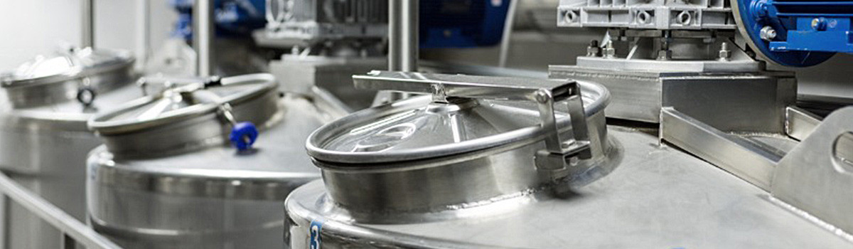
The PCB potting manufacturing process involves encapsulating printed circuit boards (PCBs) with a protective material to enhance their durability and reliability. Potting safeguards PCBs from environmental factors such as moisture, dust, and vibrations, extending their lifespan and ensuring optimal performance in various applications. This category explores the intricacies of PCB potting, covering different materials, techniques, and considerations involved in the manufacturing process.
Table of Contents
ToggleNecessary information for your knowledge:
What is PCB potting, and why is it essential in manufacturing?
PCB potting, also known as encapsulation or potting compound application, is a process crucial in manufacturing electronic devices, especially those containing printed circuit boards (PCBs). It involves filling the empty spaces, crevices, and gaps around electronic components and PCBs with a liquid resin material that solidifies into a protective shell or coating. This encapsulation offers several benefits essential in manufacturing:
- Environmental Protection: PCBs are sensitive to environmental factors like moisture, dust, chemicals, and temperature variations. Potting protects the components from these elements, ensuring reliable operation even in harsh conditions. It creates a barrier shielding sensitive electronic components from damage or corrosion.
- Mechanical Protection: Potting adds structural integrity to the electronic assembly, making it more resistant to physical shocks, vibrations, and mechanical stresses. This is particularly important in applications where the device may be subject to rough handling or frequent movement.
- Electrical Insulation: Potting compounds often have excellent electrical insulation properties. Encapsulating the components prevents electrical short circuits due to contact with conductive materials or moisture. It also reduces the risk of electromagnetic interference (EMI) and radio frequency interference (RFI), which can disrupt the proper functioning of electronic devices.
- Improved Thermal Conductivity: Some potting materials have thermal conductivity properties that help dissipate heat generated by the electronic components. By efficiently transferring heat away from critical components, potting can enhance the overall reliability and lifespan of the device, especially in applications where heat buildup is a concern.
- Chemical Resistance: Potting compounds can resist various chemicals, including solvents, oils, and fuels. This makes the encapsulated components suitable for use in environments where exposure to corrosive substances is possible.
- Enhanced Reliability: Overall, PCB potting significantly improves the reliability and longevity of electronic devices by protecting them from environmental hazards, mechanical stresses, and electrical issues. It ensures consistent performance over the device’s lifespan, reducing the likelihood of failures or malfunctions.
PCB potting is an essential manufacturing process that provides comprehensive protection to electronic components, ensuring their durability, reliability, and performance in diverse operating conditions.
What are the common materials used for potting PCBs?
Potting materials protect printed circuit boards (PCBs) from environmental hazards such as moisture, dust, vibration, and thermal stress. Commonly used materials for potting PCBs include epoxy resins, silicone, polyurethane, and acrylics.
Epoxy resins are popular for potting PCBs due to their excellent adhesive properties, chemical resistance, and mechanical strength. They provide robust protection against moisture and are relatively easy to apply. Epoxy resins come in various formulations, including rigid and flexible types, offering versatility in potting applications.
Silicone is another widely used material for potting PCBs. Silicone potting compounds offer high flexibility, thermal stability, and resistance to extreme temperatures. They also provide good electrical insulation properties, making them suitable for various electronic applications where thermal cycling concerns them.
Polyurethane potting compounds offer excellent chemical resistance and mechanical strength. They also effectively protect against moisture and vibration, making them suitable for rugged environments. Polyurethanes come in various formulations, including rigid and flexible types, allowing customization based on specific application requirements.
Acrylic resins are valued for their fast curing time and good adhesion to various substrates. They offer moderate mechanical strength and electrical insulation properties, making them suitable for potting PCBs in less demanding environments where rapid processing is essential.
Each potting material has advantages and limitations, and the choice depends on factors such as the application requirements, environmental conditions, and manufacturing constraints. Some applications may require a combination of potting materials or specialized formulations to achieve the desired level of protection and performance.
Epoxy resins, silicone, polyurethane, and acrylics are the most common materials for potting PCBs. Each material offers unique properties suited to different application needs, ensuring reliable protection and performance of electronic devices in various environments.
How does the PCB potting process enhance environmental resistance?
The PCB (Printed Circuit Board) potting process enhances environmental resistance by encapsulating electronic components and circuits within a protective material, typically epoxy resin or silicone. This process offers several key benefits that contribute to the durability and longevity of electronic devices in various environmental conditions.
Firstly, PCB potting creates a physical barrier around the components, shielding them from moisture, dust, dirt, and other contaminants that can compromise performance and reliability. By completely encapsulating the components, potting prevents the ingress of these harmful elements, reducing the risk of corrosion, short circuits, and electrical failures. This is crucial in applications exposed to harsh environments, such as outdoor installations, industrial settings, or automotive electronics.
Moreover, the potting material provides excellent insulation properties that protect against electrical interference and leakage currents. By isolating the conductive traces and components effectively, potting helps maintain signal integrity and prevent malfunctions caused by electrical shorts or interference from nearby circuits or electromagnetic fields.
Additionally, PCB potting enhances mechanical stability and shock resistance. The encapsulating material forms a rigid, protective shell around the components, reducing the risk of damage from vibration, mechanical stress, or impact. This is especially important in applications subject to rough handling, transportation, or high levels of mechanical activity.
Furthermore, PCB potting can improve thermal management by dissipating heat away from sensitive components. Many potting materials exhibit excellent thermal conductivity, allowing them to transfer heat efficiently and prevent overheating, which can degrade performance and reliability. By maintaining optimal operating temperatures, potting helps to prolong the lifespan of electronic devices and reduce the risk of thermal-related failures.
The PCB potting process is crucial in enhancing environmental resistance by providing a robust, protective barrier against moisture, contaminants, electrical interference, mechanical stress, and thermal issues. By encapsulating electronic components and circuits in a durable, insulating material, potting helps to ensure the reliability, durability, and performance of electronic devices in a wide range of challenging operating conditions.
What are the key considerations when selecting potting materials for PCBs?
Selecting potting materials for PCBs is crucial to ensure the protection and longevity of electronic components. Several key considerations must be taken into account:
- Chemical Compatibility: The potting material should be compatible with the chemicals in the environment where the PCB will be used. This prevents degradation or corrosion of the components over time.
- Thermal Conductivity: Effective dissipation of heat generated by electronic components is essential to avoid overheating and to maintain optimal performance. The potting material should have adequate thermal conductivity to dissipate heat efficiently.
- Electrical Insulation: Potting materials must provide electrical insulation to safeguard against short circuits and electrical interference. They should have high dielectric strength to prevent leakage currents and breakdown.
- Mechanical Strength: PCBs may encounter mechanical stress during handling, transportation, or operation. The potting material should possess sufficient mechanical strength to withstand these stresses and protect the delicate components from damage.
- Adhesion: Proper adhesion between the potting material and the PCB surface is crucial for ensuring uniform coverage and preventing ingress of moisture or contaminants. The material should adhere well to various substrates used in PCB fabrication.
- Thermal Stability: The potting material should maintain its properties and structural integrity over a wide temperature range, ensuring reliable performance under extreme conditions.
- Environmental Resistance: PCBs may be exposed to harsh environments like moisture, chemicals, or UV radiation. The potting material should resist these environmental factors to ensure long-term reliability and durability.
- Curing Time and Process: Considerations such as the curing time and process of the potting material should align with the PCBs’ production requirements and assembly processes, ensuring efficient manufacturing.
- Cost: Cost-effectiveness is an essential factor in material selection. The chosen potting material should meet the necessary performance requirements without significantly increasing the manufacturing cost.
By carefully considering these factors, engineers can select the most suitable potting material for PCBs, ensuring optimal protection and performance of electronic components in various applications.
What are the differences between conformal coating and potting for PCB protection?
Conformal coating and potting are methods used to protect printed circuit boards (PCBs) from environmental factors such as moisture, dust, chemicals, and physical damage. While they serve the same purpose, their application, properties, and effectiveness differ.
Conformal coating involves applying a thin layer of protective material, typically a liquid polymer, directly onto the surface of the PCB. This coating conforms to the contours of the components and circuitry, providing a barrier against moisture, dust, and other contaminants. It’s ideal for applications where the PCB needs to remain flexible or where individual components must remain accessible for repair or replacement. Conformal coatings are available in various chemistries, including acrylic, silicone, epoxy, and polyurethane, each offering different levels of protection and performance characteristics.
On the other hand, potting entails completely encapsulating the PCB and its components in a solid compound, such as epoxy resin or silicone rubber. Unlike conformal coating, potting creates a robust, three-dimensional barrier around the entire PCB assembly, offering superior protection against physical shock, vibration, and environmental hazards. Potting is particularly suitable for harsh operating conditions or applications where the PCB may be subjected to extreme temperatures, moisture, or corrosive substances. However, potting makes repairs and modifications challenging since it requires breaking through the encapsulant to access the internal components.
The main differences between conformal coating and potting lie in their application methods, level of protection, and accessibility for maintenance. Conformal coating provides a thin, flexible layer of protection that conforms to the PCB’s surface, allowing for easy access to individual components but offering less robust protection than potting. Potting, on the other hand, involves encapsulating the entire PCB assembly in a solid compound, offering superior protection against a broader range of environmental hazards but making repairs and modifications more difficult. The choice between conformal coating and potting depends on the application’s specific requirements, considering factors such as environmental conditions, accessibility, and repairability.
How does potting contribute to vibration and shock resistance in PCBs?
Potting is used in electronics manufacturing to encapsulate components, usually PCBs (Printed Circuit Boards), within a protective material such as epoxy resin or silicone. This technique significantly enhances vibration and shock resistance in PCBs through several mechanisms.
Firstly, potting creates a barrier around the PCB, shielding it from external mechanical forces. The encapsulating material absorbs and disperses energy generated by vibrations or shocks, preventing direct impact on delicate components. This cushioning effect reduces the likelihood of physical damage to the PCB and its components.
Secondly, potting reinforces the structural integrity of the PCB assembly. Filling voids and crevices eliminates spaces where components might loosen or shift under mechanical stress. This stabilization minimizes the risk of solder joint fractures or component detachment caused by vibration-induced movement.
Moreover, potting improves the PCB’s resistance to environmental factors such as moisture, dust, and chemicals. These contaminants can exacerbate vibration-induced damage by corroding exposed components or compromising their electrical connections. By sealing the PCB within a protective enclosure, potting shields it from harmful substances, enhancing its longevity and reliability in harsh operating conditions.
Furthermore, potting can dampen resonance frequencies within the PCB assembly. Resonance occurs when the natural frequency of the PCB matches the frequency of external vibrations, leading to amplified mechanical stress. Potting disrupts these resonant frequencies by adding damping material, reducing the risk of mechanical failure due to vibration-induced fatigue.
Potting contributes to vibration and shock resistance in PCBs by providing physical protection, reinforcing structural integrity, shielding against environmental hazards, and damping resonance frequencies. This technique is essential for ensuring the reliability and durability of electronic systems deployed in demanding applications such as automotive, aerospace, and industrial automation.
What are the challenges associated with potting complex PCB assemblies?
Potting complex PCB (Printed Circuit Board) assemblies involves encapsulating the electronic components within a protective material, typically epoxy or silicone. While potting offers several benefits, such as protection from environmental factors like moisture, dust, and vibration, there are several challenges associated with this process:
- Thermal Management: Potting compounds may not have the same thermal conductivity as air, leading to heat buildup within the encapsulated assembly. This could cause overheating of components, affecting their performance and lifespan.
- Compatibility: Some potting compounds may not be compatible with specific electronic components or substrates, leading to issues like corrosion or degradation over time. It’s essential to select a potting material that is compatible with all the components and materials involved.
- Curing Process: Properly curing the potting compound is crucial for its effectiveness. Factors such as temperature, humidity, and mixing ratio can influence curing. Improper curing can result in weak adhesion, voids, or uneven coverage, compromising the protection offered by potting.
- Accessibility for Repair: Once encapsulated, accessing and repairing individual components within the assembly becomes challenging. Any repairs or modifications may require the removal of the potting material, which can be time-consuming and may risk damaging the components.
- Mechanical Stress: Potting compounds must balance being rigid enough to provide adequate protection against mechanical stress and flexible enough to absorb vibrations without transferring excessive force to the components. Achieving this balance is crucial to prevent damage to delicate components.
- Cost and Time: Potting can be time-consuming and costly, especially for complex assemblies with numerous components. It involves careful planning, precise application, and often specialized equipment, all contributing to the overall cost and time required for potting.
- Quality Control: Ensuring uniform coverage and proper encapsulation of all components is essential for the reliability of the final product. Quality control measures, such as inspection techniques and testing procedures, are necessary to identify any defects or inconsistencies in the potting process.
Addressing these challenges requires a combination of careful material selection, process optimization, and thorough quality control measures to ensure the reliability and performance of potting complex PCB assemblies.
Can potting affect thermal management in PCBs?
Potting, encapsulating electronic components within a protective material, can significantly affect thermal management in printed circuit boards (PCBs). Thermal management is crucial in electronic systems to ensure reliable performance and prevent overheating, which can degrade component lifespan and functionality.
When potting is applied to PCBs, it introduces a material layer around the components, affecting their ability to dissipate heat. This layer can act as both a barrier and a medium for heat transfer, depending on the thermal conductivity of the potting material.
If the potting material has low thermal conductivity, it can hinder heat dissipation from the components to the surrounding environment, leading to increased temperatures within the PCB. This can cause components to operate at higher temperatures than intended, potentially reducing their reliability and lifespan. Additionally, localized hotspots may form, further exacerbating thermal issues.
Conversely, if the potting material has high thermal conductivity, it can facilitate heat transfer away from the components, improving thermal management. The heat generated by the components can more efficiently dissipate through the potting material to the PCB’s substrate and, ultimately, to the surroundings. This helps maintain lower operating temperatures for the components, enhancing their performance and longevity.
The choice of potting material is critical in determining its impact on thermal management. Engineers must consider factors such as thermal conductivity, coefficient of thermal expansion (CTE), adhesion properties, and compatibility with the PCB components. Additionally, the potting process must be carefully executed to avoid air voids or uneven application, which can further impede heat transfer.
Potting can significantly influence thermal management in PCBs. Proper selection of potting materials and techniques is essential to ensure efficient heat dissipation and maintain optimal operating temperatures for electronic components, enhancing system reliability and performance.
What are the steps involved in the PCB potting manufacturing process?
PCB potting, or encapsulation, involves covering electronic components and printed circuit boards (PCBs) with a protective material to shield them from environmental factors such as moisture, vibration, and mechanical shock. Here are the steps involved in the PCB potting manufacturing process:
- Component Preparation: Electronic components are mounted onto the PCB before potting according to the circuit design. This involves soldering or other attachment methods to ensure secure positioning.
- Selection of Potting Material: The appropriate potting material is chosen based on the application’s specific requirements. Factors considered include temperature range, chemical resistance, flexibility, and electrical insulation properties.
- Mixing: Potting materials often come in two parts—a resin and a hardener. These components must be mixed in the correct proportions to initiate the curing process. Mixing can be done manually or through automated equipment.
- Deaeration: Air bubbles trapped within the potting material can weaken the encapsulation and affect its effectiveness. Deaeration involves removing these bubbles through methods such as vacuum degassing or agitation.
- Encapsulation: The mixed potting material is poured or dispensed over the electronic components and PCB assembly. Care must ensure complete coverage while avoiding excess material that could lead to wastage or interference with other components.
- Curing: Once the potting material is applied, it undergoes a curing process to harden and form a protective barrier around the components. Curing can occur at ambient temperature or may require elevated temperatures depending on the specific material used.
- Post-Cure Inspection: After curing, the encapsulated PCBs undergo inspection to ensure proper potting material coverage and adherence. Any defects or imperfections are identified and addressed at this stage.
- Testing: Encapsulated PCBs are subjected to various tests to verify their functionality and reliability. This may include electrical, environmental, and performance testing to ensure they meet the required specifications.
- Packaging: Once testing is complete and the encapsulated PCBs are deemed satisfactory, they are packaged according to customer requirements for shipment and deployment in their intended applications.
By following these steps, manufacturers can produce PCB assemblies that are well-protected and capable of withstanding harsh operating conditions.
How does potting affect the electrical properties of PCBs?
Potting, also known as encapsulation or potting compound application, involves covering electronic components and printed circuit boards (PCBs) with a protective material, typically a resin, to safeguard them from environmental factors like moisture, dust, vibration, and shock. While potting is highly beneficial for enhancing the durability and reliability of PCBs, it can also affect their electrical properties in several ways.
- Dielectric Properties: The choice of potting material can significantly influence the dielectric properties of the PCB assembly. Potting compounds with high dielectric constants may alter the overall capacitance of the circuit, affecting impedance characteristics and signal propagation. This can lead to changes in circuit performance, especially in high-frequency applications.
- Insulation Resistance: Proper potting ensures insulation and protects against electrical shorts. However, inadequate potting or using materials with poor insulation properties can compromise the insulation resistance of the PCB assembly. This may result in leakage currents and potential short circuits, affecting the reliability of the electronics.
- Thermal Conductivity: Some potting materials exhibit thermal conductivity properties, which can impact the PCB’s ability to dissipate heat. Effective heat dissipation is crucial for maintaining optimal operating temperatures of electronic components. Inadequate heat dissipation due to potting can lead to overheating, degradation of components, and, ultimately, failure of the PCB.
- Conformal Coating Compatibility: Potting compounds must be compatible with conformal coatings applied to the PCB surface. Incompatibility between the potting material and conformal coating may result in adhesion issues or chemical reactions that degrade the protective layers, compromising the PCB’s reliability and longevity.
- Mechanical Stress: Improper potting can subject the PCB assembly to mechanical stress during curing or thermal expansion and contraction cycles. Excessive stress may lead to microcracks, delamination, or component displacement, potentially affecting electrical connections and overall performance.
While potting enhances PCBs’ environmental resilience, selecting appropriate materials and application techniques to mitigate any adverse effects on electrical properties is crucial. Proper consideration of dielectric properties, insulation resistance, thermal conductivity, compatibility with conformal coatings, and mechanical stress management is essential to maintain the integrity and functionality of PCB assemblies.
What are some applications that benefit from potting PCBs?
Potting or encapsulating printed circuit boards (PCBs) involves covering them with a protective material such as epoxy resin or silicone. This process offers several benefits and finds applications in various industries where electronic components are exposed to harsh environments or require additional protection.
- Electronics in Harsh Environments: PCBs used in harsh environments, such as marine, automotive, aerospace, or industrial settings, benefit significantly from potting. Encapsulation protects the PCB from moisture, chemicals, dust, and vibrations, ensuring the reliability and longevity of electronic components.
- Waterproofing: Potting is essential for applications where waterproofing is crucial, such as outdoor electronics, underwater sensors, or devices used in humid conditions. The encapsulation protects the PCB from moisture ingress, preventing corrosion and short circuits.
- Thermal Management: Encapsulating PCBs with thermally conductive materials helps dissipate heat generated by electronic components. This is particularly beneficial in high-power applications like power electronics, LED lighting, or motor drives, where efficient heat dissipation is necessary for optimal performance and reliability.
- Shock and Vibration Resistance: Potting PCBs provide mechanical reinforcement, reducing the risk of damage due to shock and vibration. This is important for applications like automotive electronics, where PCBs are subjected to constant movement and mechanical stress.
- Improved Electrical Insulation: Encapsulation enhances electrical insulation properties, reducing the risk of short circuits and electrical interference. This is critical in high-voltage applications like power supplies, inverters, or electric vehicles.
- Miniaturization: Potting enables compact and miniaturized electronic device design by protecting delicate components and reducing the need for bulky external enclosures. This benefits consumer electronics, wearables, and IoT devices where space constraints are significant.
- Environmental Protection: Encapsulating PCBs helps comply with environmental regulations by preventing the leakage of hazardous materials from electronic devices. It also enhances the recyclability and sustainability of electronic products.
- Medical Devices: In medical electronics, potting ensures the safety and reliability of electronic components in devices such as implantable medical devices, diagnostic equipment, or wearable health monitors.
Potting PCBs offer a cost-effective and reliable solution to protect electronic components in various applications. They ensure performance, durability, and safety in challenging operating conditions.
How does potting impact PCB repair and rework processes?
Potting and encapsulating electronic components or printed circuit boards (PCBs) in a protective compound can significantly impact PCB repair and rework processes. While potting offers several advantages, such as protection from environmental factors like moisture, dust, and vibrations, it also presents challenges regarding repair and rework.
One of the primary challenges of repairing or reworking a potted PCB is accessing the components buried within the encapsulant. Potting compounds are often chosen for their strong adhesion properties, making it difficult to remove them without damaging the components or the PCB itself. This means technicians may need to employ specialized tools and techniques to carefully extract components or access specific areas of the PCB for repair.
Additionally, potting compounds can hinder the visibility of components, traces, and solder joints, making it harder to diagnose issues and perform repairs accurately. Technicians may need X-ray inspection or other non-destructive testing methods to identify faults within the encapsulated PCB.
When reworking a potted PCB, technicians must also consider the thermal properties of the potting compound. Some potting materials may have high thermal conductivity, which can affect heat dissipation during rework processes such as soldering or desoldering. Excessive heat can damage sensitive components or degrade the potting material’s performance, leading to compromised protection.
Moreover, removing potting material may expose components to potential damage from mechanical stress or contamination. Careful handling and reapplication of potting material may be necessary to ensure the integrity and protection of the repaired or reworked PCB.
While potting provides valuable protection for electronic components and PCBs, it can complicate repair and rework processes due to challenges accessing components, limited visibility, thermal considerations, and careful handling to maintain protection and integrity. Technicians must employ specialized skills, tools, and techniques to effectively repair or rework potted PCBs while ensuring the reliability and performance of the final product.
What are the techniques for achieving optimal potting coverage on PCBs?
Achieving optimal potting coverage on printed circuit boards (PCBs) is crucial for ensuring electronic components’ protection, insulation, and durability. Several techniques are employed to achieve this:
- Preparation of PCB: Before potting, the PCB should be thoroughly cleaned and dried to remove contaminants or residues that may interfere with adhesion or potting compound flow.
- Fixture Design: Designing custom fixtures or molds that securely hold the PCB in place during potting ensures uniform coverage and prevents any movement that could result in uneven potting.
- Material Selection: Choosing the appropriate potting compound is critical. Factors such as viscosity, curing time, thermal conductivity, and chemical resistance should be considered based on the specific application requirements.
- Vacuum or Pressure Potting: Vacuum or pressure potting techniques help eliminate air bubbles and ensure that the potting compound fully encapsulates the PCB and components. Vacuum potting removes air from the mixture before pouring, while pressure potting applies pressure to force the potting compound into all areas of the PCB.
- Dispensing Techniques: Employing precise dispensing techniques such as robotic dispensing or meter-mix systems ensures accurate application of the potting compound, minimizing waste and achieving consistent coverage.
- Potting Process Optimization: Controlling factors like temperature, humidity, and curing time during the potting process helps optimize the flow and curing of the potting compound, resulting in better coverage and adhesion.
- Multiple Pouring Points: Using multiple pouring points strategically located across the PCB surface facilitates even distribution of the potting compound, reducing the likelihood of voids or incomplete coverage.
- Degassing: Removing trapped air from the potting compound through degassing processes before pouring prevents air pockets and ensures thorough coverage.
- Post-Potting Inspection: Conduct thorough inspections after potting to identify any areas of inadequate coverage or defects, allowing for timely corrective measures.
Manufacturers can achieve optimal potting coverage on PCBs by employing these techniques, enhancing their reliability and longevity in various electronic applications.
What are the typical curing methods used in PCB potting?
PCB potting, or encapsulation, involves filling the spaces around electronic components on a printed circuit board (PCB) with a protective material to shield them from environmental factors like moisture, vibration, and mechanical stress. Curing methods play a crucial role in potting, ensuring the encapsulant material solidifies properly to provide robust protection. Here are some typical curing methods used in PCB potting:
- Room Temperature Curing: This method allows the encapsulant material to cure at ambient temperature. Room temperature curing is convenient and doesn’t require specialized equipment. However, it can be time-consuming, often taking several hours or even days for the material to cure fully.
- Heat Curing: Heat curing involves applying heat to accelerate the curing process. This method typically involves placing the PCB assembly in an oven or using infrared lamps to heat the encapsulant material to a specific temperature. Heat curing can significantly reduce curing time, making it a preferred choice for mass production where efficiency is critical.
- UV Curing: UV curing utilizes ultraviolet (UV) light to initiate a photochemical reaction in the encapsulant material, causing it to cure rapidly. UV curing offers precise control over the process and can achieve complete curing within seconds or minutes. It is particularly suitable for encapsulating small electronic components or assemblies where heat curing may not be feasible.
- Moisture Curing: Some encapsulant materials cure in the presence of moisture from the environment or by applying moisture directly. Moisture curing can be advantageous in applications where temperature control is challenging or when rapid curing is required without requiring specialized equipment.
- Chemical Curing: Chemical curing involves using catalysts or curing agents to initiate the curing reaction in the encapsulant material. This method offers control over the curing process and can be tailored to specific application requirements, such as curing speed and final material properties.
Each curing method has advantages and limitations, and the choice depends on factors such as the encapsulant material properties, production volume, curing time requirements, and equipment availability. Manufacturers often select the most suitable curing method based on these considerations to ensure optimal performance and reliability of the potted PCB assemblies.
How does potting contribute to waterproofing PCBs?
Potting is a common technique used in electronics manufacturing to enhance the waterproofing and protection of printed circuit boards (PCBs). It involves encapsulating the electronic components and circuitry within a protective material, typically a liquid resin or silicone compound, which then cures or hardens to form a solid barrier around the components. This process provides several key benefits that contribute to waterproofing PCBs.
Firstly, potting creates a physical barrier that seals the PCB and its components from environmental elements such as moisture, dust, dirt, and chemicals. By completely encasing the electronics, potting prevents water from reaching sensitive circuitry, safeguarding against short circuits, corrosion, and other water-related damage.
Secondly, the material used for potting is often selected for its waterproof properties. For example, silicone compounds are highly water-resistant and offer excellent sealing capabilities. These materials form a tight bond with the PCB surface, filling gaps and voids to create a uniform protective layer that effectively blocks moisture.
Additionally, potting enhances the mechanical strength and durability of the PCB assembly. The hardened potting compound acts as a shock absorber, cushioning the components against mechanical stresses such as vibrations and impacts. This is particularly important in applications where the PCB may be subjected to rough handling or extreme conditions, such as outdoor electronics or industrial machinery.
Furthermore, potting can improve thermal management by dissipating heat more efficiently. Many potting compounds have good thermal conductivity properties, allowing heat generated by the electronic components to be dissipated through the potting material. This helps prevent overheating and ensures reliable operation of the PCB in harsh environments.
Overall, potting effectively waterproofs PCBs by providing a robust, protective barrier against moisture and other environmental hazards. By encapsulating the electronics in a waterproof sealant, potting helps ensure electronic devices’ long-term reliability and performance in diverse applications.
What are the considerations for potting high-frequency PCBs?
Potting high-frequency printed circuit boards (PCBs) involves encapsulating them in a protective material, typically epoxy resin, to shield them from environmental factors such as moisture, dust, and mechanical stress. However, when dealing with high-frequency PCBs, there are several considerations to keep in mind to ensure that potting does not negatively impact the electrical performance:
- Dielectric Constant (Dk) and Loss Tangent (Df): The potting material should have a low dielectric constant and loss tangent to minimize signal loss and maintain signal integrity. High Dk or Df can increase signal attenuation and distortion at high frequencies.
- Uniformity and Thickness: Ensuring uniformity in the potting material application and maintaining consistent thickness across the PCB surface is crucial. Non-uniform thickness can cause impedance variations and signal reflections, affecting high-frequency performance.
- Thermal Conductivity: High-frequency circuits can generate heat, so the potting material should have adequate thermal conductivity to dissipate heat effectively. Overheating can degrade circuit performance and reliability.
- Curing Process: The curing process of the potting material should be carefully controlled to prevent the formation of air voids or bubbles, which can introduce impedance mismatches and signal reflections.
- Compatibility with Components: Potting materials should be compatible with the components on the PCB, including sensitive high-frequency components like RF connectors and transmission lines. Some materials may interact chemically or mechanically with specific components, leading to performance degradation or failure.
- Electromagnetic Interference (EMI): Potting materials should provide sufficient shielding against EMI to prevent interference with high-frequency signals. Conductive fillers or coatings may be necessary to enhance EMI shielding effectiveness.
- Mechanical Stability: The potting material should provide mechanical stability and protection against vibrations and shocks without stressing the PCB or its components. Mechanical stress can alter the electrical characteristics of high-frequency circuits.
- Cost and Manufacturing Considerations: The choice of potting material should balance performance requirements with cost and ease of manufacturing. Some high-performance potting materials may be expensive or require specialized equipment for application.
Potting high-frequency PCBs requires careful selection and application of potting materials to maintain electrical performance while providing adequate protection against environmental and mechanical factors. Collaboration between electrical engineers, materials specialists, and manufacturing teams is essential to successfully potting high-frequency circuits.
Can potting be applied to flexible or rigid-flex PCBs?
Potting, a process of encapsulating electronic components with a resin or compound for protection, can be applied to flexible and rigid-flex PCBs. However, considerations and challenges are unique to each type of PCB construction.
Flexible PCBs, made of flexible substrate materials like polyimide, require a potting process that accommodates the material’s flexibility. Traditional potting compounds might not be suitable, as they can become rigid and compromise the PCB’s flexibility. Instead, flexible PCBs require flexible potting materials that can move and bend with the PCB without cracking or delaminating. Silicone-based potting compounds are often preferred for flexible PCBs because they maintain flexibility while providing adequate protection against environmental factors such as moisture, dust, and mechanical stress.
Rigid-flex PCBs, which combine rigid and flexible PCB elements into a single design, present a different set of challenges for potting. The transition zones between rigid and flexible sections can be susceptible to stress concentrations during potting, leading to potential damage or failure. Careful consideration must be given to selecting potting materials and the potting process to ensure uniform coverage and minimal stress on the PCB.
Additionally, the potting process for both flexible and rigid-flex PCBs requires careful planning to prevent the ingress of potting material into sensitive areas such as connectors, vias, and component interfaces. Techniques such as masking or selective potting protect these areas while providing adequate encapsulation for the rest of the PCB.
Overall, potting can be applied to both flexible and rigid-flex PCBs, but the choice of materials and the potting process must be tailored to each PCB type’s specific requirements and constraints. With proper planning and execution, potting can enhance the durability, reliability, and longevity of flexible and rigid-flex PCB assemblies in various applications.
What are the environmental regulations governing PCB potting materials?
Polychlorinated biphenyls (PCBs) are toxic chemicals that were once widely used in various industrial applications, including potting materials for electronic equipment. Due to their detrimental effects on human health and the environment, most countries have banned or heavily regulated production. Environmental regulations governing PCB potting materials typically focus on manufacturing, use, disposal, and remediation.
- Manufacturing Regulations: Many countries have banned the production of PCBs altogether or strictly regulate their manufacturing process to prevent environmental contamination. Regulations often limit PCB content in potting materials and require manufacturers to adhere to specific production standards to minimize PCB emissions.
- Use Restrictions: Regulations restrict or prohibit using PCB-containing potting materials in new electronic equipment. Instead, manufacturers are encouraged to use alternative materials that are non-toxic and environmentally friendly. This helps prevent further PCB contamination and reduces exposure risks to workers and consumers.
- Labeling and Documentation: Regulations may require proper labeling and documentation for PCB-containing potting materials still in use. This includes labeling containers with PCB content information, handling instructions, and disposal guidelines to ensure appropriate management throughout their lifecycle.
- Disposal and Remediation: Strict regulations govern the disposal of PCB-containing potting materials to prevent environmental contamination. Proper disposal methods typically involve incineration or specialized treatment facilities capable of destroying PCBs without releasing them into the environment. Remediation measures may also be required for sites contaminated with PCBs, involving cleanup efforts to mitigate environmental and human health risks.
- Monitoring and Enforcement: Environmental agencies monitor compliance with regulations governing PCB potting materials through inspections, sampling, and testing. Non-compliance can result in penalties, fines, or legal action to ensure adherence to environmental standards and protect public health.
Overall, environmental regulations governing PCB potting materials aim to minimize the release of these hazardous substances into the environment, reduce human exposure risks, and facilitate the transition to safer alternatives. Continuous monitoring, enforcement, and research into alternative materials are essential to manage and mitigate the environmental impact of PCBs effectively.
How does potting affect PCB manufacturing costs and lead times?
Potting, a process of encapsulating electronic components on a PCB with a compound like epoxy resin, can significantly affect manufacturing costs and lead times.
Firstly, in terms of costs, potting introduces additional materials and labor expenses. The cost of epoxy resin or other potting compounds adds to the overall material costs of manufacturing the PCB. Additionally, labor costs increase due to the time and expertise required for potting. Skilled technicians must carefully apply the potting compound to ensure complete coverage without damaging sensitive components. These added material and labor costs contribute to an overall increase in manufacturing expenses.
Moreover, potting can impact lead times by adding an extra step to the manufacturing process. Applying potting compounds requires additional time, often extending the overall production timeline. This can lead to longer lead times for PCB production, which may not be suitable for projects with tight deadlines. Furthermore, potting may introduce curing or drying times for the compound, further extending lead times.
Additionally, potting can introduce complexities in the assembly process. It may require equipment or specialized machinery adjustments to accommodate the potting process, leading to further delays if not adequately accounted for in the manufacturing schedule.
However, it’s important to note that while potting can increase costs and lead times, it offers benefits such as improved durability, protection against environmental factors like moisture and vibration, and enhanced thermal management. These benefits can outweigh the drawbacks for applications where reliability and longevity are paramount.
Overall, while potting adds costs and lead times to PCB manufacturing, its benefits in terms of protection and reliability may justify these additional expenses for specific applications. Manufacturers must carefully weigh these factors to determine the most appropriate approach for their needs.
What are the future trends in PCB potting technology?
PCB potting technology, a method of encapsulating printed circuit boards (PCBs) with a protective material, is witnessing several significant trends shaping its future development:
- Miniaturization and Integration: As electronics become increasingly compact and integrated, PCB potting technology must adapt to accommodate smaller form factors. Future trends will likely involve the development of potting materials that offer high levels of protection while occupying minimal space, enabling the continued miniaturization of electronic devices.
- Enhanced Thermal Management: With the growing demand for high-performance electronics, effective thermal management is crucial to prevent overheating and ensure optimal device operation. Future PCB potting materials are expected to incorporate advanced thermal management properties, such as improved heat dissipation and conductivity, to address the challenges posed by heat generation in densely packed electronic assemblies.
- Improved Environmental Sustainability: As environmental concerns become more pressing, there is a growing emphasis on developing eco-friendly potting materials with minimal environmental impact. Future trends may involve the use of biodegradable or recyclable materials in PCB potting applications, as well as the adoption of manufacturing processes that reduce energy consumption and waste generation.
- Advanced Protection Against Harsh Environments: Industries such as automotive, aerospace, and marine require electronic components that can withstand extreme temperatures, moisture, vibration, and other harsh environmental conditions. Future trends in PCB potting technology may focus on developing materials with enhanced resistance to these factors, ensuring the reliability and longevity of electronic systems in demanding operating environments.
- Integration of Smart Features: With the rise of the Internet of Things (IoT) and smart devices, there is a growing demand for PCB potting materials that integrate intelligent features such as sensors for monitoring environmental conditions or self-healing capabilities to repair minor damage automatically. Future developments may see the integration of such functionalities into potting materials, enabling enhanced functionality and reliability in IoT applications.
Overall, the future of PCB potting technology is likely to be characterized by advancements in miniaturization, thermal management, environmental sustainability, protection against harsh environments, and the integration of intelligent features, driven by the evolving needs of various industries and the ongoing technological innovations in electronics manufacturing.
Conclusion:
In conclusion, the PCB potting manufacturing process plays a crucial role in safeguarding electronic assemblies from environmental hazards, ensuring their longevity and reliability in diverse applications. By understanding the materials, techniques, and considerations involved in potting PCBs, manufacturers can effectively enhance the performance and durability of their electronic products. As technology advances, continuous innovation in potting methods is expected to further optimize PCB protection and meet the evolving demands of various industries.