Home > Potting Compound > PCB Potting Compound
PCB Potting Compound
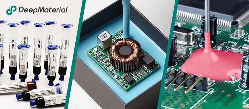
PCB potting compound plays a crucial role in protecting printed circuit boards (PCBs) from environmental factors such as moisture, dust, and vibration. It is a specialized material used for encapsulating electronic components on PCBs, ensuring their durability and reliability in various applications. This guide aims to provide comprehensive insights into PCB potting compound, its uses, benefits, and key considerations.
Table of Contents
ToggleWhat is PCB potting compound?
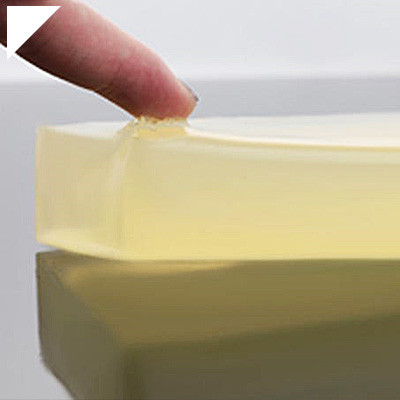
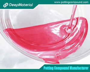
PCB potting compound, also known as encapsulation compound or potting resin, is crucial in manufacturing and protecting printed circuit boards (PCBs). Essentially, it’s a liquid or semi-liquid material poured or injected into the spaces surrounding electronic components on a PCB. Once cured, it forms a solid, protective barrier that shields the components from environmental factors such as moisture, dust, chemicals, and physical impact.
The primary purpose of using PCB potting compounds is to enhance the reliability and longevity of electronic devices. Encapsulating the sensitive components prevents them from being exposed to potentially damaging elements that could lead to malfunction or failure. Ensuring robust performance is crucial in harsh operating environments where PCBs are subjected to extreme temperatures, vibrations, or corrosive substances.
Various types of PCB potting compounds are available, each designed to meet specific application requirements. These compounds can vary in chemical composition, curing mechanism, thermal conductivity, flexibility, and resistance to environmental factors. For instance, some potting compounds are formulated to withstand high temperatures encountered in automotive or industrial applications, while others are tailored for use in marine environments where moisture and saltwater exposure are concerns.
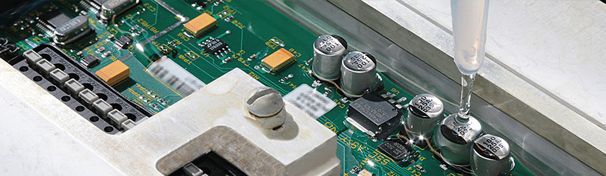
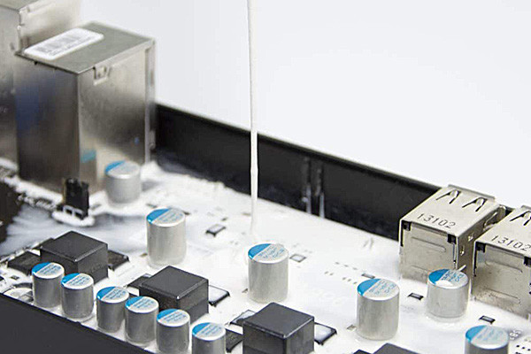
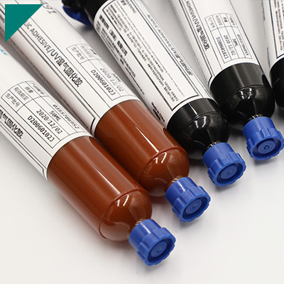
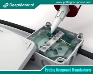
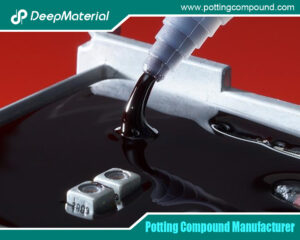
The application process of PCB potting compound typically involves mixing the components of the compound, such as resin and hardener, in the correct proportions and then pouring or injecting the mixture into the PCB assembly. Once applied, the compound undergoes a curing process, either through chemical reaction or exposure to heat, to solidify and establish a protective layer. Care must be taken during the potting process to ensure proper coverage and avoid air bubbles that could compromise the effectiveness of the encapsulation.
Overall, PCB potting compound plays a crucial role in safeguarding the integrity and reliability of electronic devices by providing a durable protective barrier against environmental hazards. Its use extends the lifespan of PCB assemblies and ensures consistent performance even in demanding operating conditions. As technology advances, developing new potting compounds with improved properties will further enhance the protection and functionality of electronic systems.
How does PCB potting compound work?
PCB potting compound works by encapsulating electronic components on printed circuit boards (PCBs), providing a protective barrier to shield against environmental factors like moisture and dust, chemicals, and vibration. Here’s how it operates:
- Encapsulation:The potting compound is applied to electronic components, surrounding them entirely or partially, forming a protective shell that seals them from external elements.
- Prevention of Corrosion:By forming a barrier against moisture and other corrosive substances, PCB potting compound helps prevent oxidation and corrosion of sensitive electronic components, prolonging their lifespan.
- Mechanical Stability:The compound enhances the mechanical stability of PCBs by providing structural support to delicate components, reducing the risk of damage from physical stress or vibration.
- Thermal Management:Some PCB potting compounds are formulated with thermal properties, dissipating heat generated by electronic components, thereby preventing overheating and ensuring optimal performance.
- Electrical Insulation:PCB potting compound acts as an electrical insulator, preventing short circuits and electrical interference by isolating conductive components from each other and external conductive materials.
- Shock Absorption:In applications subjected to mechanical shock or vibration, the potting compound absorbs and disperses energy, reducing the risk of damage to electronic components and improving overall reliability.
- Chemical Resistance:Many potting compounds resist various chemicals, protecting PCBs from exposure to harsh industrial environments or chemical spills.
- Customization:Manufacturers can tailor the properties of PCB potting compounds to meet specific application requirements, such as flexibility, hardness, or resistance to particular environmental conditions.
PCB potting compound serves as a versatile protective solution, safeguarding electronic components and PCBs from a wide range of environmental hazards while enhancing their performance, reliability, and longevity.
What are the main components of PCB potting compound?
PCB potting compounds protect printed circuit boards (PCBs) from environmental hazards, mechanical stress, and chemical exposure. Understanding the main components of these compounds is essential for engineers and manufacturers aiming to enhance the reliability and longevity of electronic devices.
Main Components of PCB Potting Compounds:
Resin:
- Epoxy:Epoxy resins are commonly used for their outstanding adhesion properties and ability to resist moisture and chemicals.
- Polyurethane:Polyurethane resins offer flexibility and durability, making them suitable for applications with varying thermal expansions.
- Silicone:Silicone resins provide high-temperature resistance and excellent electrical insulation properties, which are ideal for harsh operating conditions.
Fillers:
- Inorganic Fillers:Materials such as silica, alumina, or calcium carbonate are added to improve mechanical strength and thermal conductivity.
- Organic Fillers:Organic materials like cellulose or polyester fibers may enhance viscosity and reduce shrinkage during curing.
Curing Agents:
- Hardeners:Catalysts or curing agents initiate the chemical reaction necessary for the resin to harden into a solid state. Common examples include amines for epoxy resins and isocyanates for polyurethane resins.
- Accelerators:These additives expedite the curing process, reducing production time and improving efficiency.
Modifiers:
- Plasticizers:These compounds improve flexibility and impact resistance, which is crucial for applications exposed to mechanical stress.
- Flame Retardants:Additives such as brominated or phosphorus-based compounds enhance the fire resistance of potting compounds, ensuring compliance with safety regulations.
Considerations in Component Selection:
When selecting components for PCB potting compounds, several factors must be considered:
- Consideration of compatibility with the intended application environment is crucial, encompassing factors such as temperature extremes, humidity levels, and chemical exposure.
- Electrical characteristics, including dielectric strength, surface resistivity, and thermal conductivity, directly impact the encapsulated electronics’ performance.
- Mechanical characteristics such as hardness, flexibility, and adhesion strength ensure adequate protection against physical damage and vibration.
Understanding the composition and properties of PCB potting compounds is essential for designing robust and reliable electronic systems. By selecting the appropriate combination of resin, fillers, curing agents, and modifiers, engineers can ensure optimal performance and longevity of encapsulated PCBs in various operating conditions.
What are the advantages of using PCB potting compound?
PCB potting compound offers many benefits for electronic assemblies, ranging from enhanced protection against environmental factors to improved mechanical stability and thermal management. This versatile material encapsulates delicate components, providing a robust shield against moisture, dust, chemicals, and mechanical shocks. By mitigating the risks of premature failure due to environmental stressors and offering streamlined manufacturing processes, PCB potting compound significantly contributes to the reliability and longevity of electronic devices.
Enhanced Protection
PCB potting compound provides a robust protective barrier around electronic components, shielding them from environmental factors such as moisture, dust, chemicals, and mechanical shocks. This safeguard aids in prolonging the longevity of the PCB assembly and reduces the risk of premature failure due to environmental stressors.
Improved Mechanical Stability
By encapsulating delicate components within a solid material, PCB potting compound enhances the mechanical stability of the assembly. Preventing components from shifting or vibrating during operation reduces the risk of damage or disconnection due to mechanical stress.
Enhanced Thermal Management
Many PCB potting compounds offer excellent thermal conductivity, effectively dissipating heat generated by electronic components during operation. By efficiently managing heat, potting compound helps to prevent overheating and thermal damage, ensuring optimal performance and reliability of the PCB assembly.
Increased Resistance to Vibration
Potting compounds add a layer of damping material around components, reducing the impact of vibrations from external sources or internal movement within the assembly. This increased resistance to vibration helps to maintain the integrity of solder joints and connections, reducing the potential for failure resulting from mechanical strain.
Streamlined Manufacturing Process
Using PCB potting compound can streamline manufacturing by simplifying assembly and reducing the need for additional protective measures such as conformal coating or enclosures. Such outcomes can result in cost savings and increased efficiency during production.
Improved Electrical Insulation
Potting compounds provide excellent electrical insulation properties, lowering the possibility of electrical interference or short circuits within the PCB assembly. This insulation helps to maintain signal integrity and prevent malfunctions caused by electrical leakage or cross-talk between components.
Customization and Versatility
PCB potting compounds are available in various formulations with different properties, such as flexibility, hardness, and cure time. This flexibility allows manufacturers to select a compound that most closely matches their unique application needs, whether for automotive, aerospace, industrial, or consumer electronics.
Environmental Protection
Potting compounds help to protect electronic components from harsh environmental conditions, including moisture, chemicals, and temperature extremes. This ecological protection is precious for applications exposed to outdoor or industrial environments where reliability is critical.
Long-Term Reliability
By providing comprehensive protection against various environmental and mechanical stressors, PCB potting compound contributes to the long-term reliability of electronic assemblies. Such outcomes can lead to reduced maintenance costs, fewer warranty claims, and increased customer satisfaction over the product’s lifespan.
What are the different types of PCB potting compounds available?
PCB potting compounds protect printed circuit boards (PCBs) from environmental factors such as moisture, dust, vibrations, and temperature fluctuations. They encapsulate electronic components and provide mechanical support while ensuring electrical insulation. Understanding the various types of PCB potting compounds available is crucial for choosing the best for specific applications.
Types of PCB Potting Compounds:
- Epoxy Resins:
Epoxy resins are widely used in PCB potting due to their excellent adhesion properties, chemical resistance, and mechanical strength. They are available in different formulations, including rigid and flexible types, offering versatility in application. Epoxy resins provide robust protection against moisture and harsh environments, making them suitable for outdoor and industrial applications.
- Silicone Compounds:
Silicone potting compounds offer superior flexibility and thermal stability compared to epoxy resins. They are resistant to frigid temperatures, down to -50°C to 200°C, making them perfect for uses with frequent temperature swings or intense heat. Silicone compounds also exhibit excellent moisture, chemicals, and UV radiation resistance, ensuring long-term reliability in challenging environments.
- Polyurethane Resins:
Polyurethane potting compounds balance flexibility and rigidity, offering good shock absorption and vibration resistance. They are suitable for applications requiring impact protection and thermal cycling stability. Polyurethane resins provide excellent adhesion to various substrates, including metals, plastics, and ceramics, making them versatile for different PCB assembly processes.
- Acrylic Compounds:
Acrylic potting compounds are known for their fast cure times and low viscosity, allowing for quick and efficient potting of PCBs. They offer good electrical insulation properties and resistance to moisture and chemicals. Acrylic compounds are often chosen for applications requiring rapid processing and high-volume production due to their ease of handling and cost-effectiveness.
- Polyamide Compounds:
Polyamide potting compounds, known as nylon resins, are valued for their exceptional mechanical strength and thermal performance. They exhibit high tensile strength and resistance to abrasion, making them suitable for rugged applications subjected to mechanical stress. Polyamide compounds provide reliable protection against moisture ingress and environmental contaminants, ensuring the longevity of electronic assemblies.
The diverse range of PCB potting compounds available offers engineers and manufacturers flexibility in choosing the most appropriate solution based on specific application requirements. Whether prioritizing mechanical strength, thermal stability, chemical resistance, or ease of processing, selecting the suitable potting compound is essential for ensuring the reliability and durability of electronic assemblies in various operating conditions.
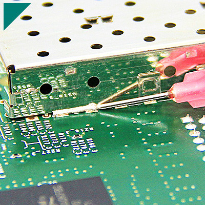
How is PCB potting compound applied to electronic components?
PCB potting compound is a crucial material used in electronic manufacturing to protect delicate components from environmental factors, mechanical stress, and chemical damage. The application of potting compounds ensures the longevity and reliability of electronic devices by encapsulating sensitive parts, such as circuit boards, integrated circuits, and connectors, in a durable protective layer. Applying PCB potting compound requires precision and expertise to achieve optimal results. Here’s an overview of how PCB potting compound is applied to electronic components:
- Preparation of Components:Before applying the potting compound, electronic components undergo thorough cleaning and preparation to remove contaminants that may hinder adhesion or compromise performance.
- Selection of Potting Compound:The appropriate potting compound is crucial, considering factors such as the operating environment, range of temperatures, chemical resistance, and mechanical qualities required for the specific application.
- Mixing and Degassing:Many potting compounds come in two-part formulations that require mixing before application. Proper mixing ratios must be maintained to ensure the compound’s effectiveness. Additionally, degassing removes air bubbles trapped in the mixture, which can compromise the integrity of the encapsulation.
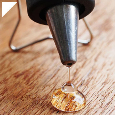
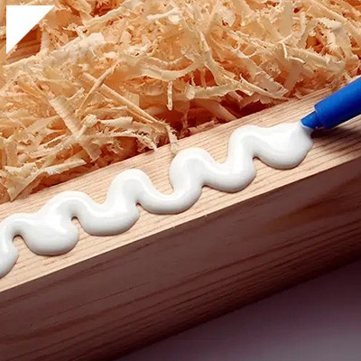
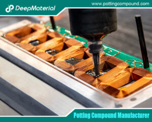
- Application Technique:A potting compound is applied using various techniques such as dipping, casting, or injection molding, depending on the size and complexity of the electronic component. Careful attention ensures complete coverage and minimal voids within the encapsulation.
- Curing Process:Once applied, the potting compound undergoes a curing process to harden and form a solid protective barrier around the electronic component. Curing methods may include air drying, oven curing, or UV curing, depending on the compound’s specifications.
- Quality Control:Throughout the application process, quality control measures are implemented to verify the proper adhesion, thickness, and coverage of the potting compound. Inspection techniques such as visual examination, x-ray imaging, or mechanical testing ensure encapsulated components meet desired performance standards.
- Post-Cure Finishing:After curing, any excess potting compound is trimmed, and the encapsulated components may undergo additional finishing processes such as labeling, marking, or conformal coating to enhance protection and identification further.
The application of PCB potting compounds to electronic components is a critical step in ensuring the reliability and longevity of electronic devices. By following precise procedures and utilizing appropriate materials, manufacturers can safeguard sensitive electronics from environmental hazards and mechanical stresses, enhancing product performance and durability.
What factors should be considered when selecting a PCB potting compound?
Selecting the suitable PCB potting compound is crucial for ensuring electronic devices’ durability, reliability, and performance. Various factors must be carefully considered to choose a potting compound that meets the application’s requirements. Here’s an overview of the critical factors to consider when selecting a PCB potting compound:
- Operating Environment:Assess the environmental conditions in which the electronic device will operate, including temperature extremes, humidity levels, exposure to chemicals, and potential mechanical stresses. Choose a potting compound resistant to these environmental factors to ensure long-term reliability.
- Chemical Compatibility:Evaluate the compatibility of the potting compound with other materials used in the device, including circuit board substrates, components, and connectors. Ensure the potting compound will not degrade or corrode these materials over time.
- Temperature Range:Consider the temperature range over which the electronic device will operate and any temperature fluctuations it may experience during everyday use or storage. Select a potting compound with a temperature rating that exceeds the device’s operating range to prevent thermal degradation and maintain performance under varying conditions.
- Mechanical Properties:Assess the mechanical stresses that the device may encounter, such as vibration, shock, or mechanical impact. Choose a potting compound with appropriate mechanical properties, including flexibility, toughness, and adhesion strength, to protect the components from damage and ensure structural integrity.
- Electrical Insulation:Verify that the potting compound provides adequate insulation to prevent short circuits and electrical leakage between components. Consider the dielectric strength, insulation resistance, and tracking resistance of the potting compound to maintain electrical reliability in the device.
- Application Method:Based on the electronic components’ size, shape, and complexity, choose the approach that will work best for the potting compound. Consider factors such as ease of application, curing time, and compatibility with existing manufacturing processes to streamline production and ensure consistent results.
- Regulatory Compliance:Ensure the selected potting compound complies with relevant industry standards and regulations, such as RoHS (Restriction of Hazardous Substances) directives, UL (Underwriters Laboratories) listings, and other certification requirements. Verify the absence of hazardous substances and potential health or environmental risks associated with the potting compound.
Selecting the appropriate PCB potting compound requires careful consideration of multiple factors to ensure compatibility with the electronic device’s operating environment, materials, and performance requirements. By evaluating these factors comprehensively, manufacturers can choose a potting compound that provides optimal product protection, reliability, and longevity.
Can PCB potting compound be customized for specific applications?
PCB (Printed Circuit Board) potting compounds protect electronic components from environmental factors like moisture, dust, vibration, and physical damage. While standard potting compounds are available in the market, customization for specific applications can offer enhanced performance and durability. One of the primary reasons for customizing potting compounds is to tailor the material properties to fulfill the particular needs of a specific application. For instance, in aerospace or automotive industries with extreme temperatures and harsh conditions, potting compounds can be customized to withstand higher temperature ranges or resist chemicals such as fuels and oils.
Customization also allows optimizing other characteristics, such as flexibility, hardness, and adhesion strength. In applications where flexibility is crucial, such as in wearable electronics or devices subject to frequent bending, a more flexible potting compound can be formulated to prevent cracking or delamination. Conversely, a more complex compound may be preferred for applications where rigidity is necessary for structural support or heat dissipation. Moreover, adhesion strength is vital to ensure the potting material adheres securely to the PCB and other components, preventing moisture ingress or mechanical failure.
Additionally, customization can address specific regulatory requirements or industry standards. For example, applications in the medical field may require potting compounds that meet biocompatibility standards to protect patients and medical personnel’s safety. Similarly, electronics used in sensitive environments such as marine or offshore installations may need potting compounds resistant to saltwater corrosion.
Overall, the ability to customize PCB potting compounds empowers manufacturers to tailor electronic components’ protection precisely to their applications’ demands, ultimately improving reliability, longevity, and performance. This customization process often involves collaboration between manufacturers, material suppliers, and end-users to identify the most suitable formulation for the intended use case.
What are the key properties to look for in a high-quality PCB potting compound?
Selecting the suitable PCB potting compound is necessary to guarantee the dependability and durability of electronic devices, particularly in demanding environments. High-quality potting compounds protect against moisture, mechanical stress, and temperature variations, safeguarding sensitive components on printed circuit boards (PCBs). Understanding the fundamental properties to look for in a high-quality potting compound is crucial for electronics manufacturers seeking optimal performance and durability for their products.
Mechanical Strength:
Another critical property to assess is the mechanical strength of the potting compound. High-quality compounds should offer sufficient structural integrity to withstand mechanical stressors like vibration, shock, and physical impact. Thermal management is especially critical in applications where electronic devices may encounter rough handling or challenging operating conditions, such as in aerospace, automotive, or industrial settings. A potting compound with high mechanical strength helps prevent damage to delicate components and ensures the continued functionality of the device.
Thermal Performance:
The thermal performance of a potting compound is vital for applications where temperature fluctuations are typical. High-quality compounds should possess excellent thermal conductivity to dissipate heat effectively and maintain optimal operating temperatures for the enclosed components. Moreover, the potting material should withstand a wide temperature range without compromising its structural integrity or adhesion to the PCB. Thermal management is crucial in telecommunications, power electronics, and LED lighting, directly impacting performance and reliability.
Electrical Insulation:
Ensuring proper electrical insulation is another fundamental property of a high-quality PCB potting compound. The material should have a high dielectric strength to prevent electrical leakage or short circuits between conductive elements on the PCB. Effective electrical insulation is essential for maintaining the integrity of electronic circuits, especially in high-voltage applications or environments prone to electrical interference. Additionally, the potting compound should be formulated to minimize the risk of corona discharge or breakdown under voltage stress, further enhancing the reliability of the encapsulated electronics.
Environmental Resistance:
Finally, high-quality PCB potting compounds should demonstrate superior environmental resistance to moisture ingress, UV exposure, and fungal growth. These properties are essential for outdoor applications, marine environments, or any setting where the electronic device may be exposed to harsh weather conditions. Choosing a potting compound with excellent environmental resistance helps prolong the service life of the encapsulated electronics and reduces the risk of premature failure due to environmental factors.
Are there any drawbacks or limitations to using PCB potting compound?
Using PCB potting compound offers numerous advantages in terms of electronic components’ protection, insulation, and durability. However, it’s essential to recognize that there are certain drawbacks and limitations associated with its use:
- Limited Accessibility for Repairs:Once the components are potted, accessing and repairing them becomes challenging, if not impossible. When maintenance or troubleshooting is necessary, the need for more clarity regarding the subject can be a significant drawback.
- Thermal Conductivity:Some potting compounds may have lower thermal conductivity compared to other materials, which can lead to heat buildup within the encapsulated components. Additional cooling mechanisms or careful consideration of the operating environment may be necessary.
- Cost Considerations:High-quality potting compounds, particularly those designed for specialized applications or environments, can be expensive. Cost can be limiting, especially for large-scale production or budget-constrained projects.
- Compatibility Issues:Not all potting compounds are compatible with every electronic component or substrate material type. It’s crucial to ensure compatibility to prevent component damage or compromised performance.
- Curing Time:Potting compounds typically require a curing period, during which the encapsulated components cannot be used. This curing time adds to the production timeline and may affect project schedules.
- Weight Addition:Potting compounds add weight to the electronic assembly, which can be a concern in applications like aerospace, where weight is crucial, or automotive industries.
- Environmental Impact:Some potting compounds may contain hazardous chemicals or materials, posing environmental concerns during manufacturing, disposal, or in the event of a breach or failure.
- Shrinkage and Expansion: During curing, some potting compounds may shrink or expand, which can affect the integrity of the encapsulation and potentially stress the components.
- Customization Challenges:Achieving the desired properties, such as flexibility, hardness, or resistance to specific environmental factors, may require custom formulations of potting compounds, which can be time-consuming and costly.
While PCB potting compounds offer significant benefits in terms of protection and reliability, it’s crucial to carefully evaluate their drawbacks and limitations to determine their suitability for specific applications. Proper selection, testing, and application are essential to mitigate potential issues and maximize the benefits of potting compounds in electronic assemblies.
What industries commonly use PCB potting compound?
PCB potting compounds find applications across various industries where electronic components require protection from environmental factors, mechanical stress, and electrical insulation. Some of the industries that commonly utilize PCB potting compounds include:
- Electronics and Telecommunications:This industry extensively relies on PCB potting compounds to safeguard sensitive electronic components such as circuit boards, sensors, and connectors from moisture, dust, and vibrations. Telecommunication equipment, ranging from base stations to satellite communication systems, often incorporates potting compounds to ensure reliable performance in diverse environmental conditions.
- Automotive:In the automotive sector, PCB potting compounds protect electronic modules and control units from harsh operating environments, including temperature variations, vibrations, and exposure to chemicals like fuels and lubricants. Potting compounds enhance the longevity and reliability of automotive electronics, contributing to vehicle safety and performance.
- Aerospace and Defense:Aerospace and defense applications demand high reliability and durability from electronic systems operating in extreme conditions. PCB potting compounds protect avionics, radar systems, navigation equipment, and military electronics from moisture, shock, and electromagnetic interference (EMI), ensuring optimal performance in critical missions and harsh environments.
- Industrial Automation:Industrial automation relies on robust electronic control systems to optimize manufacturing processes and enhance productivity. PCB potting compounds provide insulation and protection for industrial machinery’s sensors, controllers, and other electronic components. These conditions ensure reliable operation even in challenging industrial settings characterized by dust, humidity, and temperature fluctuations.
- Renewable Energy:The field of renewable energy, which encompasses wind and solar power, utilizes PCB potting compounds to protect electronic components in inverters, charge controllers, and monitoring systems. These compounds help prevent corrosion, thermal stress, and moisture ingress, prolonging the lifespan and reliability of renewable energy systems.
- Medical Devices:In the medical industry, where precision and reliability are paramount, PCB potting compounds protect electronic components in medical devices such as patient monitors, imaging equipment, and implantable devices. Potting compounds ensure the integrity of electronic assemblies in medical environments characterized by sterilization procedures, moisture, and chemical exposure.
Overall, PCB potting compounds play a crucial role in various industries where the protection and reliability of electronic components are essential for optimal performance and safety.
How does PCB potting compound contribute to the longevity of electronic devices?
PCB (Printed Circuit Board) potting compound plays a crucial role in extending the longevity of electronic devices by protecting against various environmental factors and mechanical stresses. The primary benefits of potting compounds are their ability to encapsulate electronic components on the PCB, forming a protective barrier that shields them from moisture, dust, and other contaminants. This barrier prevents corrosion and short circuits that can occur when exposed to harsh environments, thereby enhancing the reliability and durability of the device.
Moreover, the PCB potting compound helps to dissipate heat generated during electronic device operation. The compound improves thermal conductivity by filling voids and gaps around components, enabling more efficient heat transfer away from sensitive electronic parts. Effective thermal management is crucial in devices operating in high-temperature environments or those with limited airflow, as excessive heat can degrade component performance and reduce overall lifespan. By maintaining optimal operating temperatures, potting compound contributes to the prevention of thermal stress-related failures and ensures consistent performance over time.
In addition to environmental protection and thermal management, the PCB potting compound provides mechanical reinforcement to delicate components. The encapsulation process creates a solid, monolithic structure that stabilizes components and prevents them from vibrating or shifting during operation. This mechanical reinforcement reduces the risk of damage caused by shock, vibration, or other physical impacts, which can compromise the integrity of solder joints or lead to component failure. Electronic devices can withstand harsh handling or transportation conditions with enhanced mechanical stability without experiencing premature wear or failure.
Overall, the application of PCB potting compounds significantly extends the lifespan of electronic devices by addressing key reliability concerns associated with environmental exposure, thermal management, and mechanical stresses. The potting compound ensures reliable operation even in challenging operating conditions by providing a robust protective barrier, improving thermal conductivity, and enhancing mechanical stability, ultimately contributing to increased product longevity and customer satisfaction.
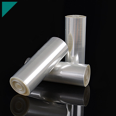
What are the differences between conformal coating and potting compound?
Conformal coating and potting compounds are both used to protect electronic components, but they differ in their application methods, properties, and intended purposes:
1. Application Method:
- Conformal Coating:Conformal coatings are typically applied as thin layers directly onto the surface of electronic circuitry. They conform to the contours of the components, forming a protective barrier against environmental factors such as moisture, dust, chemicals, and temperature extremes.
- Potting Compound:Potting compounds are typically poured or injected around electronic components, completely encapsulating them. Unlike conformal coatings, which form a thin layer, potting compounds completely encase the elements, providing more robust protection against mechanical stress, moisture ingress, and other environmental hazards.
2. Thickness and Coverage:
- Conformal Coating:Conformal coatings are thin and provide a protective layer over the surface of electronic assemblies without significantly altering their dimensions or weight. They are designed to protect while allowing for inspection, rework, and repair of components if necessary.
- Potting Compound:Potting compounds are thicker and provide complete encapsulation of electronic components. They fill all voids and crevices around the components, offering enhanced protection against physical damage, vibration, and moisture ingress. Once cured, potting compounds create a solid, durable barrier around the components.
3. Properties:
- Conformal Coating:Conformal coatings are typically flexible and resist moisture, chemicals, and temperature fluctuations. They offer good dielectric properties and can be selected based on specific requirements such as thermal conductivity, UV resistance, or flame retardancy.
- Potting Compound:Potting compounds can vary in properties depending on the application requirements. They can be formulated to provide various characteristics such as flexibility, hardness, thermal conductivity, and resistance to chemicals and environmental factors. Potting compounds offer superior mechanical strength and impact resistance compared to conformal coatings.
4. Repair and Rework:
- Conformal Coating:Conformal coatings allow for easier inspection, rework, and repair of electronic assemblies since they form a thin layer over the components. The proper solvents or mechanical methods can be used to remove them, enabling access to the underlying circuitry if needed.
- Potting Compound:Potting compounds make inspection, repair, and rework more challenging due to the complete encapsulation of components. If access to the components is required, the potting material may need to be removed entirely, which can be time-consuming and may damage the components.
Conformal coatings provide a thin, flexible protective layer over the surface of electronic assemblies while potting compounds offer complete encapsulation and robust protection against environmental hazards and mechanical stress. The choice between conformal coating and potting compound depends on factors such as the level of security required, the accessibility of components, and the specific application requirements.
Can PCB potting compound withstand extreme temperatures?
PCB potting compounds are designed to withstand a wide range of temperatures. Still, their ability to endure extreme temperatures depends on several factors, including the specific formulation of the compound and the intended application. These are some essential things to think about when the temperature resistance of PCB potting compounds:
- Formulation:The composition of the potting compound greatly influences its temperature resistance. Some formulations are engineered to withstand extreme temperatures, ranging from extremely low temperatures, such as those encountered in cryogenic environments, to high temperatures experienced in industrial processes or engine compartments.
- Thermal Conductivity:PCB potting compounds with high thermal conductivity tend to dissipate heat more effectively, which can help them withstand high temperatures by preventing heat buildup within encapsulated components.
- Glass Transition Temperature (Tg):The temperature at which glass transitions occur in the potting compound indicates the temperature at which it transitions from a rigid to a more flexible state. Compounds with higher Tg values generally offer better resistance to deformation and mechanical stress at elevated temperatures.
- Application Environment:The temperature resistance of PCB potting compounds should be evaluated based on the specific environmental conditions of the application. Factors such as ambient temperature fluctuations, exposure to heat sources, and thermal cycling can impact the potting compound’s performance over time.
- Testing and Certification:Manufacturers often conduct rigorous testing to assess the temperature resistance of PCB potting compounds under various conditions. Certifications or specifications provided by the manufacturer can indicate the temperature range over which the compound is suitable for use.
Overall, while many PCB potting compounds can withstand extreme temperatures, it’s essential to select a compound that matches the application’s temperature requirements to ensure optimal performance and reliability. Additionally, proper application techniques and adherence to manufacturer guidelines are crucial for maximizing the temperature resistance of potting compounds in electronic assemblies.
How does PCB potting compound resist moisture and environmental contaminants?
PCB potting compounds play a crucial role in protecting electronic components from moisture and environmental contaminants, guaranteeing the durability and dependability of electrical assemblies. Understanding how these compounds resist moisture and contaminants is crucial for choosing the suitable material for particular uses.
Barrier Formation:
One of the primary mechanisms by which PCB potting compounds resist moisture and environmental contaminants is barrier formation. These compounds encapsulate electronic components, creating a physical barrier that effectively seals them from water, dust, dirt, and other pollutants. By filling voids and crevices, potting compounds prevent moisture ingress and ensure the encapsulated components’ integrity.
Waterproof Properties:
Many PCB potting compounds exhibit inherent waterproof properties, further enhancing their moisture resistance. These compounds are formulated with hydrophobic additives or resin systems designed to repel water, preventing its penetration into the encapsulated components. This waterproofing capability protects sensitive electronics from water-related damage, such as corrosion and electrical short circuits.
Chemical Resistance:
In addition to moisture, PCB potting compounds are engineered to resist various environmental contaminants, including chemicals, solvents, oils, and fuels. These compounds’ chemical resistance ensures the integrity of the encapsulated components even when exposed to harsh industrial or automotive environments. By maintaining their stability in the presence of corrosive substances, potting compounds prevent degradation and prolong the lifespan of electronic assemblies.
Adhesion to Substrates:
Adequate adhesion of PCB potting compounds to substrate materials is crucial for ensuring a durable bond that enhances protection against moisture and contaminants. Proper adhesion prevents the formation of gaps or delamination between the compound and the substrate, reducing the risk of water infiltration and maintaining the encapsulation’s integrity over time.
Testing and Validation:
Manufacturers rigorously test PCB potting compounds to assess their resistance to moisture and environmental contaminants. Immersion tests, accelerated aging tests, and exposure to simulated ecological conditions are standard testing procedures used to evaluate the compound’s performance under varying scenarios. Manufacturers ensure that potting compounds meet industry standards for moisture resistance and environmental protection through comprehensive testing and validation.
Is PCB potting compound compatible with different types of electronic components?
PCB (Printed Circuit Board) potting compound is renowned for its versatility and compatibility with various electronic components. Potting compounds can effectively encapsulate and protect multiple components, whether resistors, capacitors, integrated circuits, or connectors. One of the critical advantages of potting compounds is their ability to adapt to the diverse needs of electronic assemblies, ensuring reliable performance across different applications and environments.
The compatibility of PCB potting compounds with different electronic components stems from their customizable properties. Potting compounds come in various formulations, including epoxy, silicone, and polyurethane, each tailored to specific requirements such as temperature resistance, flexibility, or chemical resistance. Because of its adaptability, engineers can choose the best potting material based on the components’ characteristics and the device’s operating conditions.
Furthermore, PCB potting compounds are designed to accommodate the thermal expansion and contraction experienced by electronic components during operation. This flexibility prevents stress buildup within the encapsulated assembly, reducing the risk of mechanical damage to delicate components such as surface-mount devices (SMDs) or microcontrollers. Additionally, some potting compounds feature low shrinkage rates upon curing, ensuring dimensional stability and minimizing the potential for stress-induced failures.
Another aspect of compatibility lies in the application process itself. Potting compounds can be dispensed via various methods, including manual potting, vacuum potting, or automated dispensing systems. This flexibility in application techniques enables precise components encapsulation, regardless of their size, shape, or orientation on the PCB. Additionally, potting compounds can be tailored to meet specific processing requirements, such as fast curing times or the ability to adhere to different substrate materials like FR4, ceramic, or flex PCBs.
In summary, PCB potting compound offers excellent compatibility with different electronic components thanks to its customizable formulations, ability to accommodate thermal expansion, and versatile application methods. Potting compounds contribute to the longevity and performance of electronic devices used for various purposes and industries by providing reliable encapsulation and protection.
What are the steps involved in the potting process?
The potting process is a crucial step in the manufacturing of electronic assemblies. It involves encapsulating components with a protective material known as a potting compound. This process ensures electronic components’ protection, insulation, and mechanical support, safeguarding them from environmental factors such as moisture, dust, vibration, and thermal stress. Understanding the steps involved in the potting process is essential for achieving consistent and reliable encapsulation of electronic assemblies.
1. Preparation of Components:
Before the potting process begins, electronic components must be prepared accordingly. Part of the process involves cleaning the components to remove any contaminants that could compromise the adhesion or performance of the potting compound. Additionally, components may need to be assembled into the desired configuration or orientation before potting.
2. Selection of Potting Compound:
The next step involves selecting the appropriate potting compound based on the application’s specific requirements. Factors such as temperature resistance, flexibility, chemical resistance, and curing time must be considered when choosing the potting material. Different formulations of potting compounds are available to suit various environmental conditions and performance criteria.
3. Mixing and Degassing:
Once the potting compound is selected, it is created by combining the ingredients for the hardener and resin according to the manufacturer’s instructions. Proper mixing ensures uniformity and consistency of the potting material. After mixing, the compound is degassed to remove any air bubbles that could weaken the encapsulation or create voids within the potting material.
4. Encapsulation of Components:
With the potting compound prepared, the encapsulation of electronic components can begin. The components are placed in a mold or fixture, and the potting compound is poured or injected around them. Care must be taken to ensure that all components are fully covered and that the encapsulation has no voids or gaps.
5. Curing and Post-Curing:
After encapsulation, the potting compound undergoes a curing process to harden and form a solid protective barrier around the electronic components. Curing conditions such as temperature, humidity, and curing time are optimized to achieve the desired properties of the potting material. Once cured, any excess material may be trimmed or removed, and the encapsulated assembly is ready for testing and integration into the final product.
How can one ensure proper curing of PCB potting compound?
Ensuring proper curing of PCB potting compound is essential to achieve optimal performance and reliability of encapsulated electronic assemblies. Here are some critical steps and considerations to ensure the adequate curing of potting compound:
- Follow Manufacturer Guidelines:Adhere to the manufacturer’s instructions and guidelines for mixing ratios, curing temperatures, curing times, and any specific curing procedures recommended for the particular potting compound.
- Controlled Environment:Maintain a controlled environment during curing, including temperature and humidity, to optimize the process. Ensure that the curing conditions align with the requirements specified by the manufacturer.
- Uniform Application:Ensure uniform application of the potting compound around the electronic components to promote consistent curing and avoid uneven material distribution. Proper mixing and degassing of the compound help prevent air bubbles and ensure uniformity.
- Avoid Overfilling:Avoid overfilling the mold or enclosure with potting compound, as excessive material can lead to longer curing times or incomplete curing. Follow recommended potting depths and fill levels specified by the manufacturer.
- Monitor Curing Progress:Monitor the curing progress closely to ensure the potting compound reaches its desired hardness and properties. Visual inspection and monitoring of temperature and curing time can help assess the progress of curing.
- Post-Curing Considerations:Some potting compounds may require post-curing procedures to achieve optimal properties. Follow any recommended post-curing steps provided by the manufacturer to enhance the performance and durability of the encapsulated assembly.
- Quality Control Testing:Conduct quality control testing, such as hardness testing, adhesion testing, and electrical testing, to verify that the potting compound has cured properly and meets the application’s requirements.
By following these steps and considerations, one can ensure proper curing of PCB potting compound, leading to robust and reliable encapsulation of electronic components for various applications.
Are there any safety considerations when working with PCB potting compound?
When working with PCB potting compounds, it’s essential to put safety first to avert possible risks and guarantee personnel’s well-being. Here are some important safety considerations to keep in mind:
- Personal Protective Equipment (PPE):Use the proper protective clothing, including goggles, gloves, and protective clothing, to minimize skin contact and inhalation of fumes or particulates.
- Ventilation:Work in a well-ventilated area or use equipment for local exhaust ventilation to reduce exposure to potentially harmful vapors or airborne particles emitted during the potting compound’s mixing, pouring, and curing.
- Chemical Handling:Handle potting compounds carefully and follow the manufacturer’s instructions for safe handling, storage, and disposal. Avoid direct contact with the eyes, skin, or mucous membranes, and wash hands thoroughly after handling.
- Avoidance of Inhalation:Avoid inhaling fumes or dust generated during the mixing and curing By utilizing the proper respiratory protection or operating in a well-ventilated space, such as respirators or masks, if necessary.
- Temperature Control:Be cautious when working with heated potting compounds or during curing, as elevated temperatures can pose burn hazards. Follow proper procedures for heating and cooling of materials to prevent accidents or thermal injuries.
- Fire Safety:Exercise caution when working with potting compounds that are flammable or combustible. Keep ignition sources away from the work area, and have fire extinguishing equipment readily available in emergencies.
- Emergency Response:Familiarize yourself with emergency procedures and protocols for handling spills, accidents, or exposure incidents involving potting compounds. Have appropriate first aid measures in place and seek medical attention if necessary.
By following these safety guidelines and taking suitable precautions, individuals can minimize risks associated with working with PCB potting compounds and ensure a safe working environment for all personnel involved.
What future developments are expected in the field of PCB potting compounds?
In the PCB (Printed Circuit Board) potting compounds, several exciting developments are anticipated to handle new issues and improve electronic gadget performance and dependability even more. One of the critical areas of focus for future growth is the formulation of environmentally friendly potting materials. As sustainability becomes increasingly important in manufacturing processes, there is a growing demand for potting compounds that prevent and lessen the usage of dangerous chemicals and the environmental impact of electronic waste. Researchers are exploring alternative materials and manufacturing techniques, such as bio-based resins or recyclable potting compounds, to meet these sustainability goals while maintaining the desired properties of protection and encapsulation.
Additionally, there is a growing need for potting compounds that can withstand more extreme operating conditions. With the ongoing development of smaller and more compact complexity, they are deployed in increasingly challenging environments, such as high-temperature, high-pressure, or corrosive settings. Future developments in potting compounds are expected to enhance mechanical strength, chemical resistance, and thermal stability to ensure reliable performance in these demanding applications. Advanced materials, such as nanocomposites or hybrid polymers, may offer enhanced properties that meet the requirements of next-generation electronic devices.
Another area of innovation in PCB potting compounds is the integration of additional functionalities beyond traditional encapsulation and protection. For example, researchers are exploring incorporating self-healing properties into potting materials to repair microcracks or damage that may occur during operation. This self-repair capability could extend the lifespan of electronic devices and reduce the need for maintenance or replacement. Furthermore, there is growing interest in developing potting compounds with embedded sensors or additives that enable real-time monitoring of environmental conditions, component performance, or structural integrity. These innovative potting materials could provide valuable insights into device health and allow predictive maintenance strategies, ultimately improving reliability and uptime.
The future of PCB potting compounds is expected to involve sustainability, performance, and functionality advancements. By developing environmentally friendly materials, enhancing resistance to extreme conditions, and incorporating additional functionalities, researchers aim to meet the electronics industry’s evolving needs and drive innovation in device design and manufacturing.
Conclusion:
PCB potting compound is a vital element in safeguarding electronic components and PCBs against environmental hazards. Its versatility, protective properties, and customization options make it indispensable across various industries. Understanding its characteristics and applications is essential for ensuring the reliability and longevity of electronic devices and systems. As technology advances, further innovations in PCB potting compounds are expected to enhance performance and address evolving industry needs.
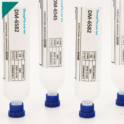
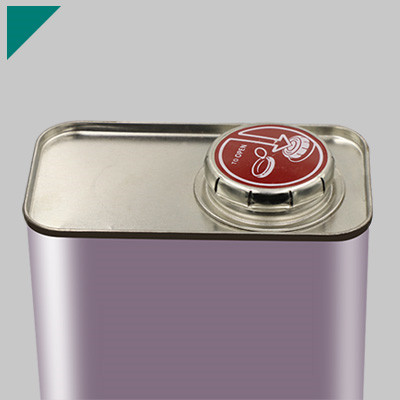
About DeepMaterial
DeepMaterial is a trusted supplier of encapsulant materials that are used in electronics manufacturing worldwide. From chip on board encapsulants such as glob top material to conformal coatings, underfills, low pressure molding, and potting solutions, DeepMaterial offers a full range of circuit board protection materials that effectively protect circuit boards while help reduce costs. More…Deepmaterial is a the manufacturer of epoxy adhesives including hardeners, metalbond, and metal filled resins. Structural, toughened medium viscosity, and non-sag adhesives are also offered. Some adhesives are resistant to thermal shock, chemical, vibration dampening, and impact. Suitable for metals, plastics, wood, and ceramics. Serves electronics, aerospace, automotive, tooling, marine, and construction industries. REACH and RoHS compliant. FDA approved. UL listed. Meets military specifications. We are the one of best adhesive manufacturers in China.
Blogs & News
Potting compounds are at the frontline of electronics assembly, delivering effective protection in challenging environmental conditions while improving mechanical strength and offering high electric insulation. Used within a variety of industries, electrical potting compounds are found within a broad range of consumer electronics, as well as used in applications across the automotive, aerospace, and other industries where electronic assemblies are prevalent.
Conformal Coating vs. Potting: What’s the Difference for Your PCB?
Conformal Coating vs. Potting: What’s the Difference for Your PCB? In the world of electronics manufacturing, the longevity of a Printed Circuit Board (PCB)
Common Mistakes to Avoid When Applying Conformal Coating
Common Mistakes to Avoid When Applying Conformal Coating In the world of electronics manufacturing, the difference between a product that lasts a decade and
How Does Potting and Encapsulation Protect Electronic Components?
How Does Potting and Encapsulation Protect Electronic Components? In an increasingly electrified and connected world, electronic components are deployed in environments ranging from the
How to Prevent Voids in Circuit Board Potting: A Comprehensive Guide to Reliable Encapsulation
How to Prevent Voids in Circuit Board Potting: A Comprehensive Guide to Reliable Encapsulation Potting, the process of encapsulating a printed circuit board (PCB)
How to Choose the Right Potting Material for Your PCB
How to Choose the Right Potting Material for Your PCB Printed Circuit Boards (PCBs) form the backbone of modern electronics, but their delicate
Basic Knowledge, Methods and Materials about Electronic Encapsulation
Basic Knowledge, Methods and Materials about Electronic Encapsulation In an era defined by ubiquitous electronics—from the smartphone in your pocket to the sensor monitoring