How To Remove Potting Material From A PC Board
Potting material can be a formidable obstacle when it comes to repairing or salvaging components from a printed circuit board (PCB). Whether you’re dealing with epoxy, silicone, or other encapsulating agents, knowing the right techniques to remove potting material without damaging the underlying PCB is crucial. In this comprehensive guide, we’ll explore various methods and tools for safely and effectively removing potting material, ensuring that you can tackle this challenge with confidence.
Fundamental concepts you must comprehend:
What is potting material, and why is it used on PCBs?
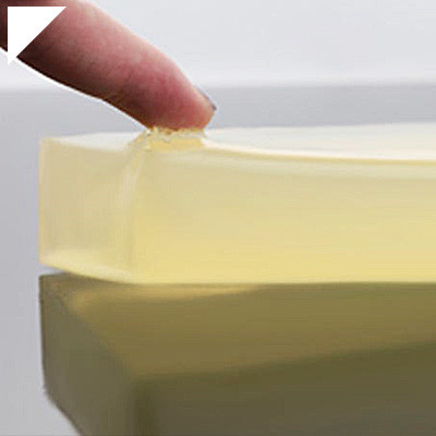
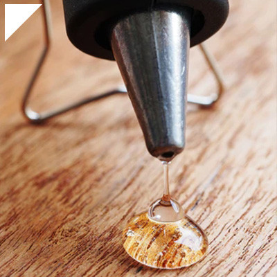
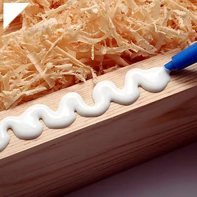
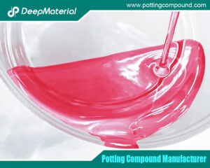
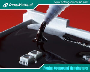
Potting material, also known as encapsulant or potting compound, is a substance used to protect electronic components and circuitry on printed circuit boards (PCBs). It is typically a resin-based material that is poured, injected, or applied in a liquid form and then solidified to form a protective barrier around the components.
The primary purpose of potting material on PCBs is to provide environmental protection. Electronic components are often sensitive to environmental factors such as moisture, dust, chemicals, and mechanical stress. Exposure to these elements can lead to corrosion, short circuits, and other forms of damage, compromising the functionality and reliability of the circuitry. Potting material forms a barrier that shields the components from these environmental factors, extending their lifespan and enhancing performance.
Furthermore, potting material enhances the mechanical stability of PCBs. It helps to immobilize the components and prevent them from vibrating or moving due to mechanical shocks or vibrations. This is particularly important in applications where the PCBs are subjected to rough handling, such as in automotive, aerospace, or industrial environments.
Potting material also provides thermal insulation and heat dissipation properties. It helps distribute heat generated by the electronic components more evenly, preventing hot spots and thermal stress that could degrade the components’ performance. Additionally, some potting compounds have excellent thermal conductivity, further enhancing heat dissipation and improving the PCB’s overall thermal management.
Moreover, potting material can offer electrical insulation, protecting the components from electrical interference and reducing the risk of short circuits or electrical leakage.
Potting material plays a crucial role in protecting and enhancing the performance of PCBs by providing environmental protection, mechanical stability, thermal management, and electrical insulation. It is an essential part of the manufacturing process for electronic devices and is used across various industries to ensure the reliability and durability of electronic systems.
What are the common types of potting material encountered on PCBs?
Potting materials are used in electronics manufacturing to encapsulate and protect components, particularly on printed circuit boards (PCBs). These materials serve various purposes, including insulation, preventing moisture ingress, enhancing mechanical strength, and resisting environmental factors like chemicals and temperature fluctuations. Several common types of potting materials encountered on PCBs include:
- Epoxy Resins: Epoxy resins are widely used for potting due to their excellent electrical insulation properties, adhesion strength, and chemical resistance. They come in various formulations, including rigid and flexible types, making them suitable for different applications.
- Polyurethanes (PU): PU potting compounds offer flexibility, impact resistance, and thermal stability. They are often chosen for applications requiring vibration damping or thermal cycling resistance. PU potting materials come in different hardness levels to accommodate varying requirements.
- Silicone: Silicone potting compounds are known for their broad temperature range capability, excellent flexibility, and resistance to moisture and chemicals. They are commonly used in harsh environments where temperature extremes or exposure to moisture is a concern. Silicone materials also exhibit good electrical insulation properties.
- Acrylics: Acrylic potting materials provide good adhesion to various substrates and decent electrical insulation properties. They are often chosen for applications requiring transparency or clarity, as acrylics can be formulated to be optically transparent.
- Polyesters: Polyester-based potting compounds offer good electrical insulation properties and mechanical strength. They are typically chosen for applications where cost-effectiveness is a priority, although they may offer a smaller temperature range or chemical resistance than other materials.
- Polyamide (Nylon): Polyamide potting materials provide good moisture, chemical resistance, and high-temperature tolerance. They are commonly used in applications where thermal stability and chemical resistance are critical.
- Parylene: Parylene coating is a unique potting method where a thin, conformal layer of Parylene polymer is deposited onto the PCB surface. It offers excellent moisture barrier properties, dielectric strength, and chemical resistance while maintaining flexibility and transparency.
Each type of potting material has its own set of properties and is chosen based on the application’s specific requirements, such as environmental conditions, mechanical stresses, and electrical insulation needs. The selection process involves considering factors such as temperature range, flexibility, adhesion, and cost-effectiveness to ensure optimal performance and reliability of the PCB assembly.
What are the risks of improper potting material removal?
Improper removal of potting material can pose several risks, particularly when electronic components or delicate structures are involved. Here are some of the key risks:
- Damage to Components: Potting materials protect electronic components from moisture, shock, and vibration. Improper removal can lead to physical damage to these components, such as cracked circuit boards, broken wires, or dislodged parts. This damage can render the device inoperable or decrease its reliability.
- Electrical Short Circuits: Inadequate removal of potting material can leave behind residue or debris that may cause electrical short circuits. Conductive materials or metallic particles left within the device can create unintended pathways for electrical current, leading to malfunction, overheating, or even fire hazards.
- Degradation of Performance: Potting materials are designed to provide insulation and mechanical support to electronic components. Improper removal may compromise the insulation properties, leading to decreased performance or reliability of the device. This can result in erratic behavior, signal interference, or data corruption.
- Voiding of Warranties: Tampering with potting materials without proper expertise or authorization can void warranties manufacturers provide. If the device requires servicing or repair, manufacturers may refuse to honor warranties due to evidence of unauthorized modification, leading to additional costs for the owner.
- Health and Safety Risks: Some potting materials contain hazardous chemicals or emit harmful fumes when disturbed or heated. Improper removal without adequate precautions can expose individuals to health risks such as respiratory irritation, allergic reactions, or chemical burns. Proper safety measures, including personal protective equipment and ventilation, are essential when dealing with such materials.
- Loss of Intellectual Property: Potting materials may protect sensitive designs or proprietary technology in industrial or proprietary applications. Improper removal can expose these intellectual assets to competitors or unauthorized parties, leading to intellectual property theft or loss of competitive advantage.
Improper removal of potting material can result in various risks, including damage to components, electrical hazards, performance degradation, warranty voidance, health and safety concerns, and loss of intellectual property. Therefore, following proper procedures and seeking expert guidance when handling potting materials is crucial to effectively mitigate these risks.
How does potting material affect PCB repair and salvaging efforts?
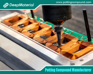
Potting material is often used in electronic devices to encapsulate components, and it presents unique challenges in PCB (Printed Circuit Board) repair and salvaging efforts. The potting material is typically a resin-based compound poured over electronic components to protect them from environmental factors such as moisture, vibration, and physical damage. While this provides excellent protection during the device’s lifespan, it complicates repair processes due to its insulating and adhesive properties.
Firstly, potting material impedes access to components and solder joints on the PCB. The resin encapsulates the elements, making identifying, accessing, and desoldering individual parts difficult. This complicates repair efforts as technicians often use destructive methods to access the components, potentially damaging the PCB or adjacent elements.
Secondly, potting material acts as a thermal insulator, exacerbating heat-related issues during repair. When attempting to desolder components, the heat required to melt solder may be insufficient due to the potting material’s insulating properties. This can prolong the repair process, increase the risk of overheating sensitive components, or even damage the PCB.
Additionally, the adhesive nature of potting compounds can make it challenging to remove the material without causing damage. Traditional methods, such as scraping or heating, may not be effective and can risk further harm to the PCB or components. Specialized tools and techniques, such as chemical solvents or mechanical milling, may be necessary to remove the potting material safely.
Despite these challenges, potting material also serves as a protective barrier, preserving components from environmental damage. This protection can be advantageous in salvaging efforts as it may prevent corrosion or physical degradation of valuable components, increasing the likelihood of successful salvage.
Potting material poses significant challenges in PCB repair and salvaging efforts due to its insulating, adhesive, and protective properties. Technicians must employ specialized tools and techniques to overcome these challenges while minimizing the risk of damage to the PCB and components. Additionally, careful consideration should be given to the trade-offs between preserving the protective benefits of potting material and its difficulties in repair and salvage operations.
What safety precautions should be taken before attempting to remove potting material?
Before attempting to remove potting material from a PCB, it’s crucial to prioritize safety to protect both the technician and the integrity of the components. Here are several safety precautions to consider:
- Personal Protective Equipment (PPE): Wear appropriate PPE, including safety glasses or goggles to protect your eyes from debris, chemical-resistant gloves to shield your hands from potential irritants or solvents, and a respirator or mask if working with potentially harmful fumes or dust.
- Ventilation: Ensure adequate ventilation in the work area to prevent the buildup of fumes or airborne particles generated during removal. This may involve working in a well-ventilated room or using fume extraction equipment to remove harmful vapors.
- Chemical Handling: If using chemical solvents to soften or dissolve the potting material, carefully read and follow the manufacturer’s instructions for safe handling, storage, and disposal of the chemicals. Use chemical-resistant containers and avoid contact with skin or eyes.
- Fire Safety: Some potting materials may be flammable, especially when exposed to heat sources such as soldering irons or hot air rework stations. Keep fire extinguishing equipment nearby and be cautious when using heat around potentially explosive materials.
- Electrical Safety: Before beginning the removal process, ensure the PCB is disconnected from any power source to prevent electrical shock hazards. If working on live circuits is necessary, take appropriate precautions, such as using insulated tools and gloves.
- Tool Safety: Use tools appropriate for the task and handle them carefully to avoid injury. Sharp tools such as knives or chisels should be used cautiously to prevent cuts or punctures, and power tools should be operated according to safety guidelines to avoid accidents.
- Work Surface Protection: Protect the work surface from damage or contamination using suitable materials such as disposable mats or non-reactive trays. This helps prevent accidental spills or scratches to the PCB or surrounding equipment.
By adhering to these safety precautions, technicians can mitigate risks and ensure a safe working environment while attempting to remove potting material from a PCB. Additionally, it’s advisable to consult with experienced professionals or refer to manufacturer guidelines for specific safety recommendations related to the potting material used.
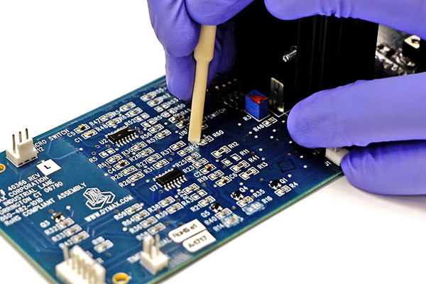
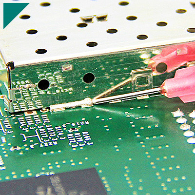
What tools are essential for removing potting material from a PCB?
Removing potting material from a printed circuit board (PCB) can be a delicate and challenging task, requiring precision and care to avoid damaging the components or the board itself. Potting material is typically used to encapsulate and protect electronic components from environmental factors such as moisture, vibration, and heat. However, there are situations where the potting material needs to be removed for repair, maintenance, or component replacement purposes. Essential tools for this task include:
- Heat Gun or Heat Plate: Applying heat to the potting material softens it, making removing it easier. A heat gun or heat plate allows controlled heating of the potting material without damaging the components on the PCB. Care must be taken to avoid overheating, which can cause damage to the board or components.
- Chemical Solvents: Some potting materials may require chemical solvents for softening or dissolving. Typical solvents include acetone, isopropyl alcohol (IPA), or commercially available potting material removers. These solvents help to break down the potting material, making it easier to remove without damaging the PCB or components.
- Precision Tools: Various precision tools such as tweezers, dental picks, or small chisels are essential for carefully chipping away or prying off the softened potting material around the components. These tools enable precise and controlled removal while minimizing the risk of damage to the PCB or components.
- Safety Equipment: Safety goggles, gloves, and a well-ventilated workspace are crucial when working with heat guns, chemical solvents, and potentially hazardous potting materials. Proper safety equipment protects against injury and exposure to harmful fumes or substances.
- Brushes and Compressed Air: Once the potting material is softened and removed, brushes and compressed air can be used to clean any residue or debris from the PCB surface and components. This ensures a clean working environment and prevents contaminants from affecting the functionality of the PCB.
- Magnifying Glass or Microscope: A magnifying glass or microscope can aid in inspecting the PCB for any damage or residue that may have been missed during the removal process. This allows for thorough examination and ensures the integrity of the PCB before reassembly or further repairs.
By employing these essential tools and taking appropriate precautions, technicians can effectively remove potting material from PCBs while minimizing the risk of damage and ensuring the integrity of the components and the board itself.
What are the steps involved in preparing a PCB for potting material removal?
Preparing a printed circuit board (PCB) for potting material removal involves several crucial steps to ensure the safe and efficient removal of the potting compound without damaging the PCB or its components. Here are the steps involved:
- Assessment and Planning:Before starting the removal process, assess the PCB to determine the type of potting material used and the components it encapsulates. Plan the removal process accordingly, considering factors such as the type of potting material, component sensitivity, and desired outcome.
- Safety Precautions:Wear appropriate personal protective equipment (PPE) such as gloves, safety goggles, and a mask to protect against potential hazards associated with the potting material and any chemicals used in the removal process.
- Heat Application:Apply controlled heat to soften the potting material. This can be done using a heat gun or an oven set to a specific temperature based on the potting material’s melting point. Heat helps to soften the material, making it easier to remove without damaging the PCB or components.
- Mechanical Removal:Once the potting material has softened, use non-destructive methods such as scraping, brushing, or using specialized tools to remove the softened material from the PCB surface. Carefully scrape away the potting compound layer by layer, ensuring it does not damage the underlying components or traces on the PCB.
- Chemical Solvents (if applicable):In some cases, chemical solvents may be necessary to dissolve or weaken the potting material further. Select a solvent compatible with the potting material and the PCB components. Apply the solvent cautiously and follow proper safety guidelines to avoid damaging the PCB or causing harm.
- Cleaning and Inspection:After removing the potting material, thoroughly clean the PCB to remove any residue or debris left behind. Inspect the PCB and its components for any signs of damage or contamination. Repair any damaged traces or components as needed before proceeding further.
- Post-Processing:Once the PCB is clean and free from potting material, perform any necessary post-processing steps, such as reapplication of protective coatings or conformal coatings, to ensure the PCB’s longevity and reliability.
By following these steps carefully, you can effectively prepare a PCB for potting material removal while minimizing the risk of damage to the board or its components.
What is the best method for determining the type of potting material on a PCB?
Determining the type of potting material on a printed circuit board (PCB) is crucial for various reasons, including maintenance, repair, and compliance requirements. While there isn’t a one-size-fits-all method, several approaches can help identify potting materials effectively.
- Visual Inspection: A visual examination can provide initial clues about the potting material. Different potting materials have distinct appearances, textures, colors, and levels of transparency. Observing these characteristics under appropriate lighting conditions can offer valuable insights.
- Chemical Testing: Chemical testing involves using solvents or reagents to interact with the potting material and observing the reaction. For instance, some potting materials dissolve or soften in specific solvents, which can help identify their composition. However, this method requires caution to ensure the PCB’s integrity isn’t compromised.
- Thermal Analysis: Thermal analysis techniques such as thermogravimetric analysis (TGA) or differential scanning calorimetry (DSC) can aid in identifying the potting material based on its thermal behavior. Each material has a unique thermal profile, including melting points, decomposition temperatures, and heat capacities, which can be compared against known data.
- Microscopic Examination: Microscopic examination using techniques like scanning electron microscopy (SEM) or optical microscopy can provide detailed insights into the potting material’s structure, morphology, and composition at a microscopic level, aiding in its identification.
- FTIR Spectroscopy: Fourier-transform infrared spectroscopy (FTIR) can be utilized to analyze the potting material’s chemical composition by measuring its absorption of infrared radiation. Each material exhibits characteristic absorption bands, allowing for identification based on spectral analysis.
- X-Ray Diffraction (XRD): XRD is a technique used to analyze the crystalline structure of materials. By subjecting the potting material to X-ray radiation, its crystallographic structure can be determined, aiding in material identification.
- Consultation with Manufacturers or Suppliers: If the PCB was manufactured externally, contacting the manufacturer or supplier for information regarding the potting material used can provide valuable insights, especially if detailed records were maintained.
Combining multiple methods often yields the most accurate results, as each approach has limitations and strengths. Additionally, employing experienced professionals with expertise in materials analysis can enhance the effectiveness of the identification process.
How can heat be used to soften potting material for removal?
Heat can effectively soften potting material for removal through a process known as thermal decomposition or softening. This technique is commonly employed in various industries such as electronics, automotive, and aerospace to extract or replace components embedded in potting compounds or epoxy resins. Here’s how heat can be utilized for this purpose:
- Thermal Expansion: When subjected to heat, potting materials undergo thermal expansion. This expansion causes the material to loosen its grip on embedded components, making them easier to remove. As the temperature increases, the bonds holding the potting material weaken, facilitating the extraction process.
- Softening Point: Most potting materials begin to soften at a specific temperature. Heating the potting material to or slightly above this temperature makes it more pliable and easier to manipulate. This softening point varies depending on the composition of the potting material, with thermosetting resins typically requiring higher temperatures than thermoplastics.
- Thermal Degradation: Excessive heat can lead to thermal degradation of the potting material. When subjected to temperatures beyond their tolerance limits, the material’s molecular structure breaks down, resulting in a loss of mechanical strength and viscosity. This degradation facilitates the removal of the softened material, either through manual extraction or mechanical tools.
- Localized Heating: Targeted or localized heating methods are sometimes employed to soften potting material. Techniques such as heat guns, infrared lamps, or induction heating can apply heat directly to the desired area, allowing precise control over the softening process. This approach minimizes the risk of damage to surrounding components and facilitates selective removal of potting material.
- Safety Considerations: It’s crucial to exercise caution when applying heat to potting materials, especially in environments where flammable or toxic fumes may be generated. Adequate ventilation and personal protective equipment should be utilized to mitigate potential hazards associated with thermal decomposition or overheating of the potting material.
Heat can be effectively employed to soften potting material for removal by exploiting principles such as thermal expansion, softening points, thermal degradation, localized heating, and ensuring safety measures are in place to manage potential risks.
What are the advantages and disadvantages of using heat to remove potting material?
Using heat to remove potting material, such as epoxy or resin, from electronic components or devices offers advantages and disadvantages.
Advantages:
- Efficiency: Heat-based methods typically expedite the removal process compared to mechanical methods. The application of heat softens the potting material, making it easier to separate from the components. This can save time and labor, especially when dealing with large batches of components.
- Preservation of components: Heat can be applied and controlled, minimizing the risk of damage to the electronic components embedded within the potting material. Unlike mechanical methods that may involve scraping or chipping away at the material, heat allows for a gentler approach, reducing the likelihood of component damage.
- Versatility: Heat-based removal techniques can be adapted to various potting materials, including epoxies, resins, and silicones. This versatility makes heat a widely applicable method for depopulating electronic assemblies.
- Cost-effectiveness: While specialized equipment may be necessary for heating the potting material, the overall cost of heat-based removal methods can be relatively low compared to other techniques. Additionally, the efficiency of heat-based methods can contribute to cost savings in terms of labor and time.
Disadvantages:
- Temperature control: Excessive heat can damage sensitive electronic components or lead to thermal stress within the assembly. Therefore, precise temperature control is crucial to prevent overheating and ensure the integrity of the components.
- Safety concerns: Working with heat poses inherent safety risks, including the possibility of burns, fires, or the release of toxic fumes from overheated potting materials. Proper safety precautions, such as using protective equipment and working in well-ventilated areas, are essential when employing heat-based removal methods.
- Environmental impact: Some potting materials may release harmful emissions when subjected to high temperatures, contributing to environmental pollution. Proper disposal methods should be employed to mitigate these environmental concerns.
- Limited effectiveness: Heat-based methods may only suit some potting materials or configurations. Some materials may require alternative techniques for efficient removal, necessitating additional time and resources.
While heat-based removal methods offer efficiency, component preservation, versatility, and cost-effectiveness, they also come with challenges such as temperature control, safety concerns, environmental impact, and limitations in effectiveness. Careful consideration of these factors is essential when deciding whether to utilize heat for potting material removal in electronic assemblies.
Can chemical solvents effectively dissolve potting material, and what precautions are necessary when using them?
Chemical solvents can effectively dissolve potting material, typically consisting of resins, adhesives, or encapsulating compounds used to protect electronic components. Typical solvents include acetone, isopropyl alcohol (IPA), methyl ethyl ketone (MEK), and toluene. These solvents break down the molecular bonds within the potting material, allowing it to be dissolved or softened for removal.
However, when using chemical solvents for dissolving potting material, several precautions must be taken:
- Ventilation: Ensure proper ventilation in the workspace to prevent the buildup of solvent vapors, which can be harmful if inhaled. Use fume hoods or work in well-ventilated areas.
- Personal Protective Equipment (PPE): Wear appropriate PPE such as gloves, goggles, and a respirator to protect against skin contact, eye irritation, and inhalation of solvent fumes.
- Compatibility: Check the solvent’s compatibility with the potting material and the substrate to which it’s adhered. Some solvents may damage certain materials, so it’s crucial to verify compatibility before use.
- Fire Hazard: Many solvents are flammable, posing a fire hazard. Keep solvents away from ignition sources and handle them cautiously to prevent accidents.
- Storage: Store solvents in properly labeled containers in a cool, dry place away from direct sunlight and heat sources. Follow all safety instructions provided by the manufacturer.
- Disposal: Dispose of used solvents according to local regulations. Many solvents are hazardous waste and require special disposal procedures to prevent environmental contamination.
- Spills and Leaks: Clean up spills and leaks promptly using appropriate absorbent materials. Avoid allowing solvents to contact skin, clothing, or other materials.
- Safety Data Sheets (SDS): Familiarize yourself with the SDS for the solvent you are using. It contains important information about hazards, safe handling procedures, and emergency measures.
By following these precautions, chemical solvents can effectively dissolve potting material while minimizing risks to health and safety. Proper handling and awareness of potential hazards are essential for a safe working environment.
Are there any environmentally friendly solvents for potting material removal?
Removing potting material while considering environmental impact necessitates the use of eco-friendly solvents. Several options exist, each with varying degrees of effectiveness and environmental friendliness. One such solvent is limonene, a natural compound derived from citrus fruits. Limonene exhibits strong solvency properties and is biodegradable, making it a favorable choice for environmentally conscious applications. Additionally, it has a pleasant citrus scent, unlike many conventional solvents, which can be harsh and harmful.
Another eco-friendly solvent option is soy-based solvents. These solvents are derived from soybeans and contain low volatile organic compounds (VOCs), reducing their environmental footprint. Soy-based solvents offer effective potting material removal while being renewable and biodegradable.
Furthermore, terpenes, organic compounds in various plants, can serve as environmentally friendly solvents. Terpenes such as pinene and terpinolene demonstrate excellent solvency characteristics and are non-toxic. These solvents are derived from natural sources and can be easily broken down by biological processes, minimizing environmental harm.
Bio-based solvents from renewable resources like ethanol or ethyl lactate offer environmentally friendly alternatives for removing potting material. These solvents are low-toxicity and readily biodegradable, reducing their environmental impact.
Moreover, supercritical carbon dioxide (CO2) extraction presents a unique eco-friendly solvent option. It utilizes carbon dioxide in a state that combines the properties of both a liquid and a gas, allowing it to act as a solvent for removing potting material. CO2 is non-toxic, non-flammable, and readily available, making it an attractive option for environmentally friendly solvent applications.
Several environmentally friendly solvents exist for potting material removal, ranging from natural compounds like limonene and terpenes to bio-based solvents like soy-based solutions and ethanol. Innovative methods such as supercritical CO2 extraction offer sustainable alternatives with minimal environmental impact. Choosing these eco-friendly solvents promotes responsible ecological stewardship while effectively meeting the needs of potting material removal processes.
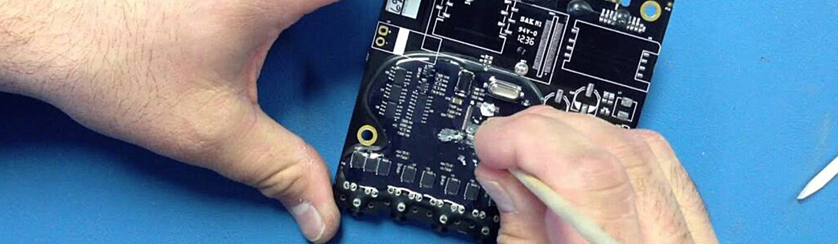
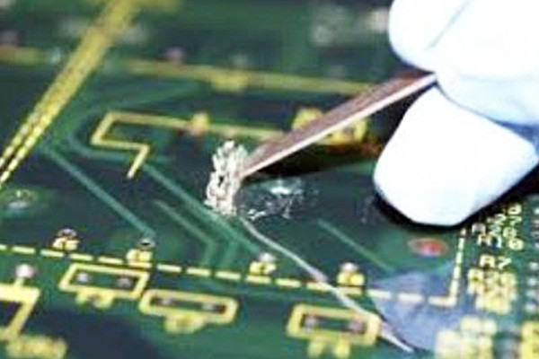
How does mechanical removal of potting material work, and what tools are used for this method?
Mechanical removal of potting material is employed to extract electronic components or devices from their enclosures, such as potting compounds or resins, without damaging the elements. Potting materials are commonly used in electronics to protect sensitive components from environmental factors like moisture, dust, and vibration. However, during repair, maintenance, or recycling processes, it becomes necessary to remove these materials without harming the components.
The mechanical removal process typically involves the following steps:
- Assessment: Before initiating the removal process, technicians assess the potting material type used and the enclosed components. This helps determine the appropriate method and tools required for extraction.
- Preparation: Components may need to be heated or cooled to facilitate easier removal of the potting material. Heat guns, soldering irons, or freeze sprays can be used for this purpose.
- Mechanical Extraction: Once prepared, technicians use various mechanical tools to chip away or cut through the potting material carefully. Commonly used tools include:
- Chisels and Scrapers: These are used to chip away at the potting material gradually, allowing access to the components underneath. They come in various shapes and sizes to suit different applications.
- Precision Knives: Razor blades or precision knives are employed to carefully slice through the potting material without damaging the enclosed components.
- Dremel Tools: Rotary tools equipped with cutting or grinding attachments can be used to remove potting material from around components precisely.
- Ultrasonic Cutters: These tools use ultrasonic vibrations to break down potting material, making it easier to remove without causing damage to the components.
- Cleanup: Once the potting material is removed, any residue left on the components is cleaned off using solvents or mechanical means, ensuring the components are ready for further testing, repair, or recycling.
- Inspection: Finally, the components are inspected for any damage incurred during removal. Any necessary repairs or replacements are carried out before reassembly or reuse.
Overall, mechanical removal of potting material requires precision, patience, and appropriate tools to ensure the integrity of the enclosed components is maintained throughout the process.
What are the risks of mechanical removal, and how can they be mitigated?
Mechanical removal, whether in surgery, engineering, or any other field, poses several risks that must be carefully managed to ensure safety and effectiveness.
- Tissue Damage: One of the primary risks of mechanical removal in surgery is accidental damage to surrounding tissues. This can lead to bleeding, nerve damage, or organ perforation. Mitigation involves thorough pre-operative planning, precise instruments, and the expertise of skilled surgeons to minimize collateral damage.
- Infection: Any breach of the body’s natural barriers increases the risk of infection. Mechanical removal procedures create entry points for pathogens. Sterile techniques, proper wound care, and prophylactic antibiotics can mitigate this risk.
- Complications: Complications such as blood clots, excessive bleeding, or allergic reactions to anesthesia can arise during or after mechanical removal procedures. Close monitoring during the procedure and post-operative care helps identify and address complications promptly.
- Scarring and Disfigurement: Improper technique or healing can lead to unsightly scars or disfigurement, particularly in cosmetic surgeries or dermatological procedures. Precise incisions, suturing techniques, and appropriate wound management can minimize scarring.
- Functional Impairment: Mechanical removal in certain areas, such as joints or nerves, can impair function if not performed correctly. Careful planning, imaging guidance, and rehabilitation protocols are essential for preserving function.
- Equipment Failure: Mechanical removal often relies on specialized tools and equipment. Equipment failure during the procedure can pose significant risks to the patient and the surgical team. Regular maintenance, quality assurance checks, and having backup equipment on hand help mitigate this risk.
- Anesthesia Risks: Anesthesia carries its risks, including allergic reactions, respiratory complications, and cardiovascular issues. Thorough pre-operative assessments, appropriate patient selection, and vigilant monitoring during anesthesia administration help minimize these risks.
- Psychological Impact: Particularly in cosmetic or reconstructive procedures, there’s a risk of psychological distress or dissatisfaction with the outcomes. Clear communication between the patient and the healthcare team, along with realistic expectations setting, can help mitigate this risk.
While mechanical removal procedures offer valuable therapeutic benefits, they also entail inherent risks. Mitigating these risks requires a multidisciplinary approach involving careful planning, precise execution, vigilant monitoring, and proactive management of potential complications.
Is it possible to reuse or recycle potting material after removal?
Yes, it is possible to reuse or recycle potting material after removal, depending on the type of material and its condition. Potting materials typically include soil, peat moss, perlite, vermiculite, and various organic or synthetic amendments. Here’s how each component can be reused or recycled:
- Soil can be reused after removal from pots by revitalizing it through composting or amending it with organic matter to replenish nutrients. Sterilizing the soil by heating it in an oven or exposing it to sunlight can also kill pathogens and weed seeds, making it suitable for reuse. Additionally, soil can be incorporated into garden beds or used as a top dressing for existing plants.
- Peat Moss: Peat moss is a common component in potting mixes due to its ability to retain moisture. While it’s not renewable and harvesting, it can have environmental impacts; peat moss can be composted to enrich the soil or mixed with other organic materials to create a nutrient-rich substrate for planting.
- Perlite and Vermiculite: These lightweight, porous materials are added to potting mixes to improve drainage and aeration. Perlite and vermiculite can be washed and sterilized for reuse in new potting mixes. Alternatively, they can be incorporated into garden soil to enhance its structure and drainage capacity.
- Organic Amendments: Organic materials such as compost, coconut coir, and composted bark contribute to the fertility and structure of potting mixes. After removal from pots, these amendments can be composted to create nutrient-rich soil amendments or used as mulch to suppress weeds and retain moisture in garden beds.
- Synthetic Materials: Some potting mixes contain synthetic additives like water-absorbing polymers or slow-release fertilizers. While these materials may not be suitable for reuse, they can often be recycled through specialized programs offered by waste management facilities or manufacturers.
Reusing or recycling potting materials can help reduce waste, conserve resources, and promote sustainable gardening practices. However, it’s essential to assess the condition of the materials and ensure they are free from contaminants before repurposing them in new gardening projects.
What are some common challenges encountered during potting material removal, and how can they be overcome?
Potting material removal, particularly in electronics or manufacturing processes, can present several challenges that require careful consideration and technique to overcome:
- Adhesion: Potting materials often adhere firmly to encapsulating components or surfaces. This adhesion can make removal difficult and may risk damaging delicate parts. To overcome this challenge, using appropriate solvents or mechanical methods such as scraping or chiseling can help weaken the bond between the potting material and the surface.
- Complex Geometry: Components with intricate shapes or densely packed assemblies can make accessing and removing potting material uniformly challenging. Utilizing specialized tools such as miniature drills, needles, or ultrasonic equipment can aid in reaching confined spaces and ensuring thorough removal without causing damage.
- Heat Sensitivity: Some electronic components are sensitive to heat, making traditional methods like heat guns or soldering irons unsuitable for potting material removal. In such cases, employing low-temperature techniques like freeze sprays or controlled thermal methods can mitigate the risk of damaging sensitive parts while facilitating material removal.
- Environmental Concerns: Potting materials may contain hazardous substances, posing environmental and health risks during removal. Proper safety measures, such as working in well-ventilated areas and using personal protective equipment, are crucial to minimize exposure to harmful fumes or particles.
- Residue Cleanup: After removing the potting material, residue often remains on the components or surfaces, interfering with subsequent processes or compromising performance. Thorough cleaning using appropriate solvents, brushes, or specialized cleaning equipment is essential to ensure the complete removal of residue and restore the integrity of the components.
- Time and Cost: Potting material removal can be time-consuming and labor-intensive, impacting production schedules and increasing operational costs. Employing efficient methods, optimizing workflow processes, and investing in specialized equipment or automation where feasible can help mitigate these challenges and streamline the removal process.
By addressing these common challenges with careful planning, appropriate techniques, and adherence to safety protocols, manufacturers can effectively remove potting material while preserving the integrity of their components and minimizing operational disruptions.
Can freezing techniques aid in potting material removal, and if so, how are they applied?
Freezing techniques can help remove potting material, especially when the material is adhered firmly to the potted object. These techniques are instrumental when dealing with epoxy or resin-based potting compounds that tend to form strong bonds with surfaces. Subjecting the potting material to freezing temperatures alters its physical properties, making it more brittle and more accessible to remove.
One standard method involves using liquid nitrogen or dry ice to cool the potting material rapidly. Liquid nitrogen has a temperature of around -196°C (-321°F), while dry ice, which is solid carbon dioxide, has a temperature of -78.5°C (-109.3°F). Both substances can quickly reduce the temperature of the potting material and the surrounding area.
Liquid nitrogen or dry ice is typically placed near the potting material to apply freezing techniques. Liquid nitrogen can be poured directly onto the material or applied using a spray bottle. Dry ice can be wrapped in cloth or placed in a container and positioned near the potting material. The objective is to lower the temperature of the potting material as quickly as possible.
As the potting material cools, it becomes more brittle, contracting and losing its adhesive properties. This makes it easier to chip away or pry off from the object being potted. Additionally, the contraction of the material can create microfractures, further facilitating its removal.
However, it’s essential to exercise caution when using freezing techniques, especially with liquid nitrogen, as it can cause severe frostbite upon contact with the skin. Proper protective gear should be worn, and safety protocols must be followed.
Freezing techniques can be highly effective for removing potting material by making it more brittle and accessible to manipulate. These methods can save time and effort compared to traditional removal techniques, especially in cases where the potting material forms strong bonds with surfaces.
Are there any specialized techniques for removing potting material from delicate or sensitive components?
Removing potting material from delicate or sensitive components requires careful handling to avoid damage. Potting compounds such as epoxy or silicone are commonly used to protect electronic components from environmental factors like moisture, dust, and vibrations. However, removing the potting material can be challenging when these components need to be repaired or replaced. Here are some specialized techniques for safely removing potting material:
- Heat Gun or Hot Air Station: Applying controlled heat using a heat gun or hot air station can soften the potting material without damaging the sensitive components. The heat softens the potting compound, making removing it easier without causing stress to the components.
- Chemical Solvents: Certain chemical solvents can dissolve potting compounds without harming the underlying components. However, selecting a solvent that won’t damage the components is crucial, and ensuring proper ventilation and safety precautions are followed when working with chemicals.
- Mechanical Methods: Delicate scraping or precision cutting tools can sometimes be employed to remove potting material carefully. This method requires a steady hand and a keen eye to avoid damaging the components.
- Ultrasonic Cleaning: Ultrasonic cleaning can remove potting material from small, delicate components. The high-frequency vibrations generated by ultrasonic cleaners help to break down and dislodge the potting compound without causing damage to the components.
- Freezing: In some cases, freezing the potting material can make it more brittle and more accessible to remove. Once frozen, the potting compound can be carefully chipped away using precision tools.
- Softening Agents: Certain softening agents or debonding agents are specifically designed to weaken the bond between the potting material and the components, making it easier to remove the potting material without causing damage.
- Laser Ablation: In highly specialized cases, laser ablation can selectively remove potting material layer by layer. This precise technique requires specialized equipment and expertise but can be incredibly effective for removing potting material without damaging delicate components.
Regardless of the method chosen, it’s essential to proceed with caution and test any technique on a small, inconspicuous area before applying it to the entire assembly. Also, proper protective equipment should always be worn, and best practices for component handling should be followed to prevent damage during the removal of potting material.
How can one ensure the cleanliness of the PCB after potting material removal?
Cleaning a printed circuit board (PCB) after potting material removal is crucial to ensure its proper functionality and longevity. Potting compounds protect electronic components from moisture, dust, and mechanical stress. Still, they can leave residues that must be removed to prevent electrical shorts, corrosion, or interference with soldering. Here’s how to ensure the cleanliness of the PCB after potting material removal:
- Visual Inspection: Before cleaning, visually inspect the PCB to identify any residues, debris, or damaged components resulting from the potting material removal process. This step helps in planning the cleaning strategy and ensures thoroughness.
- Selection of Cleaning Agent: Choose an appropriate cleaning agent based on the type of potting material used and the PCB’s components. Common cleaning agents include isopropyl alcohol (IPA), acetone, or specialized electronic cleaners. Ensure compatibility with the PCB materials to avoid damage.
- Application Method: Apply the chosen cleaning agent using a suitable method, such as spraying, immersion, or brushing. Ensure even coverage across the PCB surface and focus on areas where residues are prominent, such as component leads or tight spaces.
- Mechanical Agitation: Gentle mechanical agitation may be necessary for stubborn residues. Use soft brushes, cotton swabs, or non-abrasive pads to dislodge residues without damaging the PCB or components. Exercise caution to prevent accidental dislodging of sensitive components.
- Rinsing: After cleaning, rinse the PCB thoroughly with clean, deionized water to remove any remaining cleaning agent and loosened residues. Ensure complete rinsing to prevent residue redeposition or chemical reactions affecting performance.
- Drying: Allow the PCB to dry completely before further handling or assembly. Compressed air or a low-temperature oven to accelerate drying, ensuring no moisture remains trapped in components or crevices.
- Inspection and Testing: After cleaning and drying, another visual inspection is performed to confirm cleanliness. Additionally, electrical testing must be conducted to ensure that the PCB functions correctly and that no residues are causing electrical issues.
- Protective Coating (Optional): Consider applying a conformal coating to the PCB after cleaning to protect against environmental factors such as moisture, dust, and chemical exposure.
By following these steps carefully, one can ensure the cleanliness of the PCB after potting material removal, promoting optimal performance and reliability in electronic applications.
What are some tips for troubleshooting issues during potting material removal processes?
Troubleshooting potting material removal processes can be challenging, but a systematic approach can help identify and address issues efficiently. Here are some tips:
- Understand the Material: Familiarize yourself with the potting material’s properties. Different materials may require different removal techniques based on their composition, viscosity, and curing mechanisms.
- Inspect Equipment: Check equipment such as potting machines, molds, and removal tools for any signs of damage or wear that could affect the removal process. Ensure they are appropriately calibrated and maintained.
- Review Process Parameters: Evaluate parameters such as temperature, pressure, and curing time used during potting. Deviations from optimal conditions could affect the ease of material removal.
- Consider Environmental Factors: Environmental conditions like humidity and ambient temperature can influence the potting material’s properties and removal. Adjustments may be needed to compensate for these factors.
- Assess Adhesion: Determine the level of adhesion between the potting material and the substrate. Weak adhesion may indicate improper surface preparation or contamination, while strong adhesion may require more aggressive removal techniques.
- Troubleshoot Removal Techniques: Experiment with different removal techniques such as mechanical scraping, chemical solvents, heat, or specialized tools like laser ablation. Identify which method works best for the specific potting material and substrate combination.
- Optimize Tooling: Ensure removal tools are appropriately selected and configured. Consider factors such as tool material, geometry, and abrasiveness to minimize damage to the substrate while effectively removing the potting material.
- Implement Safety Measures: Follow safety protocols when handling removal tools and chemicals. Provide adequate ventilation and personal protective equipment to mitigate risks associated with specific removal techniques.
- Document Findings: Keep detailed records of troubleshooting efforts, including observations, interventions, and outcomes. This documentation can be a reference for future troubleshooting and process improvement efforts.
- Seek Expert Advice: If troubleshooting efforts prove challenging, don’t hesitate to consult with colleagues, equipment manufacturers, or material suppliers for additional guidance and support.
Following these tips and maintaining a systematic approach can effectively troubleshoot potting material removal processes and ensure smooth operations in your manufacturing or assembly environment.
Conclusion:
Removing potting material from a PCB requires careful planning, the right tools, and a good understanding of the material properties. By following the techniques outlined in this guide and taking appropriate safety precautions, you can successfully navigate the challenges associated with potting material removal, ultimately enhancing your ability to repair and salvage electronic components effectively.
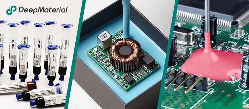
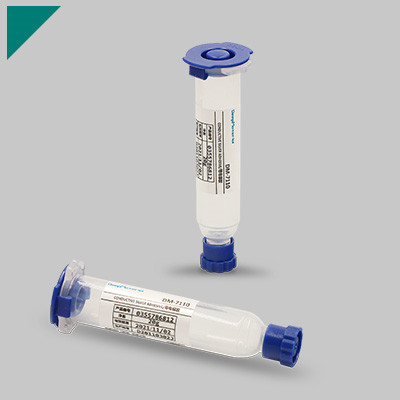
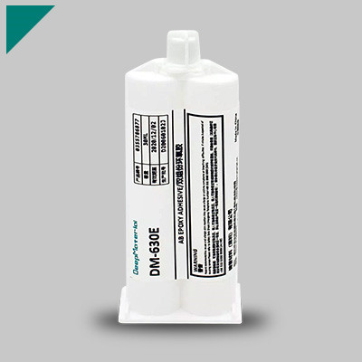
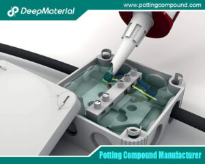
About DeepMaterial
DeepMaterial is a trusted supplier of encapsulant materials that are used in electronics manufacturing worldwide. From chip on board encapsulants such as glob top material to conformal coatings, underfills, low pressure molding, and potting solutions, DeepMaterial offers a full range of circuit board protection materials that effectively protect circuit boards while help reduce costs. More…Deepmaterial is a the manufacturer of epoxy adhesives including hardeners, metalbond, and metal filled resins. Structural, toughened medium viscosity, and non-sag adhesives are also offered. Some adhesives are resistant to thermal shock, chemical, vibration dampening, and impact. Suitable for metals, plastics, wood, and ceramics. Serves electronics, aerospace, automotive, tooling, marine, and construction industries. REACH and RoHS compliant. FDA approved. UL listed. Meets military specifications. We are the one of best adhesive manufacturers in China.
Blogs & News
Potting compounds are at the frontline of electronics assembly, delivering effective protection in challenging environmental conditions while improving mechanical strength and offering high electric insulation. Used within a variety of industries, electrical potting compounds are found within a broad range of consumer electronics, as well as used in applications across the automotive, aerospace, and other industries where electronic assemblies are prevalent.
Conformal Coating vs. Potting: What’s the Difference for Your PCB?
Conformal Coating vs. Potting: What’s the Difference for Your PCB? In the world of electronics manufacturing, the longevity of a Printed Circuit Board (PCB)
Common Mistakes to Avoid When Applying Conformal Coating
Common Mistakes to Avoid When Applying Conformal Coating In the world of electronics manufacturing, the difference between a product that lasts a decade and
How Does Potting and Encapsulation Protect Electronic Components?
How Does Potting and Encapsulation Protect Electronic Components? In an increasingly electrified and connected world, electronic components are deployed in environments ranging from the
How to Prevent Voids in Circuit Board Potting: A Comprehensive Guide to Reliable Encapsulation
How to Prevent Voids in Circuit Board Potting: A Comprehensive Guide to Reliable Encapsulation Potting, the process of encapsulating a printed circuit board (PCB)
How to Choose the Right Potting Material for Your PCB
How to Choose the Right Potting Material for Your PCB Printed Circuit Boards (PCBs) form the backbone of modern electronics, but their delicate
Basic Knowledge, Methods and Materials about Electronic Encapsulation
Basic Knowledge, Methods and Materials about Electronic Encapsulation In an era defined by ubiquitous electronics—from the smartphone in your pocket to the sensor monitoring