Phone: +86-133 5263 6504
Phone: +86-133 5263 6504
A Comprehensive Analysis of PCB Encapsulation Quality Inspection: Innovative Application of Non-Destructive Testing Technologies
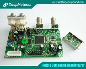
In the field of electronic manufacturing, the encapsulation process of printed circuit boards (PCBs) plays a crucial role in protecting electronic components and enhancing their stability and reliability. Encapsulated PCBs are widely used in high-reliability fields such as automotive electronics, aerospace, and industrial control. For example, in the engine control unit of a car, the encapsulated PCB can resist harsh environments such as high temperatures, vibrations, and humidity, ensuring the stable operation of the automotive electronic system. With the development of electronic products towards miniaturization and high performance, higher requirements have been put forward for the inspection of PCB encapsulation quality. This article will deeply explore the inspection methods for the encapsulation quality of PCBs after encapsulation, with a focus on introducing non-destructive testing technologies.
Importance of PCB Encapsulation and Common Quality Issues
(A) Key Roles of Encapsulation
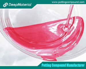
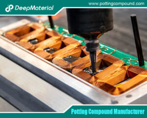
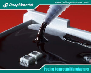
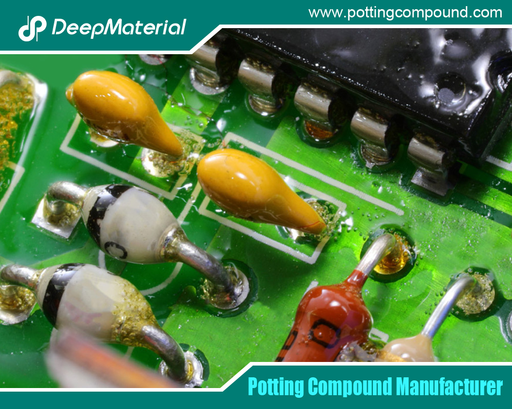
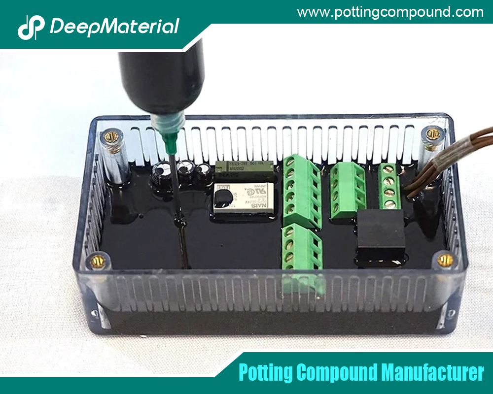
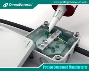
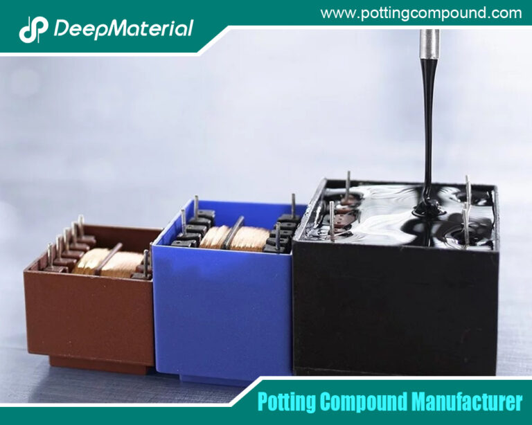
Encapsulation is the process of filling a specific area of the PCB with liquid encapsulation material, which forms a protective coating or sealing body after curing. This process mainly has the following functions: Firstly, it provides physical protection, preventing components from being affected by mechanical impacts, vibrations, dust, etc. Secondly, it enhances the electrical insulation performance, avoiding short circuits between components with different potentials. Thirdly, it helps with heat dissipation, effectively transferring the heat generated by components during operation to ensure they operate at an appropriate temperature. Fourthly, it protects against the erosion of chemical substances, enabling the PCB to work normally in environments with the risk of chemical corrosion.
(B) Common Quality Issues
- Bubble Problems: If air is mixed in during the encapsulation process, bubbles will form within the encapsulation body. These bubbles not only reduce the mechanical strength of the encapsulation material but may also affect the electrical performance. In a high-voltage environment, partial discharge is likely to occur at the location of the bubbles.
- Void Problems: Voids usually appear at the solder joints or at the interface between the components and the encapsulation material. They may be caused by insufficient wettability of the encapsulation material, curing shrinkage, etc. In severe cases, they can lead to open circuits or poor soldering, affecting the connectivity of the circuit.
- Crack Problems: After the encapsulation material is cured, cracks may occur under the action of temperature changes, mechanical stress, etc. Cracks will destroy the integrity of the encapsulation, leaving the internal components unprotected and thus reducing the reliability of the PCB.
- Delamination Problems: Delamination may occur between the encapsulation material and the PCB or the surface of the components. This is mainly due to reasons such as insufficient surface cleaning and poor material compatibility, resulting in insufficient adhesion between the two. Delamination will weaken the protective effect of the encapsulation.
Traditional Testing Methods and Their Limitations
(A) Visual Inspection
- Testing Method: The encapsulated PCB surface is directly observed with the naked eye or with the help of tools such as magnifying glasses and microscopes. The inspection content includes the surface flatness of the encapsulation material, the presence of bubbles, cracks, impurities, as well as the neatness of the encapsulation boundary and whether it covers the designated area.
- Limitations: It can only detect surface-visible defects and cannot detect internal hidden defects such as bubbles, voids, and delamination. Moreover, the test results are greatly affected by the experience and subjective judgment of the inspectors. Different inspectors may have different inspection standards, making it difficult to ensure the consistency and accuracy of the inspection.
(B) Physical Performance Testing
- Testing Method
- Hardness Testing: A hardness tester, such as a Shore hardness tester, is used to test the encapsulation material. By measuring the ability of the encapsulation material to resist indentation, the hardness of the material can be determined to see if it meets the requirements.
- Tensile Strength and Compressive Strength Testing: A materials testing machine is used to apply tensile or compressive forces to the encapsulated samples, and the tensile strength and compressive strength are measured to evaluate the performance of the encapsulation material under stress.
- Thermal Performance Testing: Thermal analyzers, such as differential scanning calorimetry (DSC) and thermogravimetric analysis (TGA), are used to test the thermal performance parameters of the encapsulation material, such as the glass transition temperature and thermal decomposition temperature, to understand its stability under different temperature conditions.
- Limitations: It requires the destruction of samples for testing, and it is impossible to comprehensively test the finished products. Only a small number of samples can be taken for destructive testing, and it cannot be guaranteed that the quality of the untested products is qualified. Moreover, the testing process is relatively complicated, the testing cycle is long, and the cost is high, making it unsuitable for rapid testing in large-scale production.
(C) Electrical Performance Testing
- Testing Method
- Insulation Resistance Testing: An insulation resistance tester is used to apply a certain voltage to the encapsulated PCB, and the insulation resistance between different conductive parts is measured to determine whether the insulation performance of the encapsulation material is good.
- Withstand Voltage Testing: Through a withstand voltage tester, a gradually increasing voltage is applied to the PCB until the specified withstand voltage value is reached, and it is observed whether there are phenomena such as breakdown and leakage to detect the electrical safety of the encapsulated PCB in a high-voltage environment.
- Limitations: It can only indirectly reflect the encapsulation quality. If an abnormal electrical performance is detected, it is difficult to accurately determine whether it is caused by an encapsulation quality problem or a fault in other circuit components. Moreover, for some potential encapsulation defects that have not yet affected the electrical performance, they cannot be detected in a timely manner.
Non-Destructive Testing Methods and Their Advantages
(A) X-ray Detection Technology
- Detection Principle: Based on the fact that when X-rays penetrate an object, substances with different densities absorb X-rays to different degrees. When testing an encapsulated PCB, X-rays penetrate the encapsulation material, components, and PCB substrate. Metals with a higher density (such as solder joints) absorb X-rays more strongly and appear as darker areas in the imaging; while materials with a lower density (such as bubbles and voids in the encapsulation material) absorb X-rays weakly and appear as brighter areas. By analyzing the X-ray images, internal defects can be detected.
- Application Examples: When detecting BGA (Ball Grid Array Package) solder joints, X-ray detection can clearly show internal voids, poor soldering, and other problems in the solder joints. In the inspection of PCB encapsulation in automotive electronics, it can effectively detect solder joint defects caused by poor encapsulation, ensuring the reliability of the automotive electronic system.
- Advantages: It does not require sample destruction, and the entire PCB can be comprehensively inspected. It can detect internal hidden defects with high detection accuracy and can detect tiny bubbles and voids. The detection speed is fast, making it suitable for on-line detection in large-scale production, and it can provide real-time feedback on the detection results, which is convenient for timely adjustment of the production process.
(B) Ultrasonic Detection Technology
- Detection Principle: Utilizes the reflection, refraction, and attenuation characteristics of ultrasonic waves when they propagate in different media. When ultrasonic waves are transmitted into the encapsulated PCB, when they encounter the interfaces of different media (such as the interface between the encapsulation material and the components, and defects in the encapsulation material), reflection and refraction will occur. By receiving and analyzing the reflected ultrasonic signals, it is possible to determine whether there are defects and the location and size of the defects.
- Application Examples: In the inspection of PCB encapsulation in the aerospace field, ultrasonic detection can be used to detect delamination and debonding problems inside multi-layer PCBs, ensuring the high reliability of avionics equipment.
- Advantages: It is sensitive to internal defects and can detect tiny delamination and debonding problems, and the detection results are not affected by the surface shape and color of the sample. The detection process is fast and convenient, and it can achieve rapid scanning detection of large PCBs. It can obtain rich internal structure information without destroying the sample.
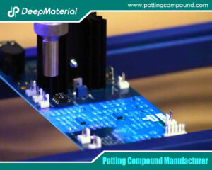
(C) Infrared Thermography Detection Technology
- Detection Principle: Based on the correlation between the surface temperature distribution of an object and its internal structure and defects. When the PCB is working, due to the passage of current and the heating of components, normal parts and parts with defects (such as bubbles, voids, and poor soldering) will generate different heat distributions. The infrared thermography imager captures the infrared radiation on the surface of the object and converts it into a temperature image, thereby discovering abnormal temperature areas and determining whether there are encapsulation quality problems.
- Application Examples: In the inspection of PCB encapsulation in the industrial control field, infrared thermography detection can be used to detect PCBs after long-term operation, discover local overheating problems caused by poor encapsulation, and prevent equipment failures in advance.
- Advantages: It can be detected when the PCB is in operation, and its operating status can be monitored in real-time. It can quickly scan a large area and quickly discover potential encapsulation quality problems. The detection process is non-contact and will not cause any damage to the PCB. The operation is simple, and the detection efficiency is high.
Selection and Application Strategies of Non-Destructive Testing Methods
(A) Select Testing Methods According to Product Characteristics
- For Small and Simple-Structured PCBs: If the requirement for detection accuracy is not particularly high, infrared thermography detection can be given priority. It is easy to operate, has a fast detection speed, and can quickly screen out obvious encapsulation quality problems.
- For PCBs with Complex Packaging Components Such as BGA: X-ray detection is the preferred method, which can clearly detect internal defects in solder joints and ensure the connection reliability of complex packaging components.
- For Multi-Layer PCBs or Products Sensitive to Defects Such as Delamination and Debonding: Ultrasonic detection is more suitable, which can effectively detect internal delamination and debonding problems and ensure the overall structural integrity of the PCB.
(B) Combine Multiple Testing Methods
In actual production, a single testing method often cannot comprehensively detect all encapsulation quality problems. Therefore, multiple non-destructive testing methods are usually combined to give full play to their respective advantages. For example, first use infrared thermography detection for preliminary screening to quickly find the possible problem areas; then use X-ray detection or ultrasonic detection for detailed testing of these suspicious areas to accurately determine the type, location, and size of the defects. Through the complementarity of multiple methods, the accuracy and reliability of the detection can be greatly improved.
(C) Establish a Complete Detection Process
- Preparation Before Detection: Calibrate and debug the detection equipment to ensure that the equipment is in the best working condition. Prepare the PCB samples to be detected and ensure that the sample surface is clean and free of impurities and contaminants.
- Detection Process: Carry out the detection according to the selected detection method and process, and strictly control the detection parameters, such as the voltage and current of the X-ray, and the frequency and power of the ultrasonic wave. Record and analyze the detection data in real-time and discover abnormal situations in a timely manner.
- Post-Detection Processing: According to the detection results, mark and release the qualified PCBs; for the unqualified PCBs, analyze the defect causes in detail, formulate improvement measures, and conduct re-detection on the improved products to ensure that the quality meets the requirements.
Conclusion
With the continuous development of electronic technology, the requirements for PCB encapsulation quality are getting higher and higher. Traditional testing methods have certain limitations and are difficult to meet the needs of modern electronic manufacturing. Non-destructive testing methods, such as X-ray detection, ultrasonic detection, and infrared thermography detection, have the advantages of being non-destructive, efficient, and accurate, and are playing an increasingly important role in the inspection of PCB encapsulation quality. In practical applications, appropriate detection methods should be selected according to product characteristics, and a complete detection process should be established by combining multiple methods to ensure PCB encapsulation quality, improve the reliability and stability of electronic products, and promote the high-quality development of the electronic manufacturing industry.
For more about a comprehensive analysis of PCB encapsulation quality inspection: innovative application of non-destructive testing technologies, you can pay a visit to DeepMaterial at https://www.pottingcompound.com/ for more info.