Phone: +86-133 5263 6504
Phone: +86-133 5263 6504
Analysis of the Improvement of the Seismic and Impact Resistance Performance of PCB by Encapsulation
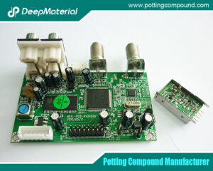
During the operation of electronic devices, the PCB (Printed Circuit Board), as the support for electronic components and the provider of electrical connections, plays a crucial role in ensuring the stability of the devices. However, PCBs often have to face various complex working environments, among which vibration and impact are important factors affecting their performance and reliability. Encapsulation, as a commonly used protection method, plays a key role in enhancing the seismic and impact resistance performance of PCBs. This article will delve into the specific improvement effects of encapsulation on the seismic and impact resistance performance of PCBs as well as the related principles.
Challenges of Vibration and Impact Faced by PCBs
In numerous application scenarios, PCBs will encounter different degrees of vibration and impact. In the field of automotive electronics, during the driving process of a vehicle, the PCB will experience continuous vibrations due to the road conditions, and strong impacts will occur during sudden braking, acceleration, or collisions. In industrial automation equipment, the running components such as motors and fans inside will also cause vibrations. Aerospace equipment will face even more severe vibration and impact environments during takeoff, flight, and landing stages.
These vibrations and impacts can cause serious harm to PCBs. From the perspective of components, they can lead to the cracking of solder joints, interrupting the electrical connection between the electronic components and the PCB, and triggering equipment failures. They can also cause the fatigue fracture of component pins. Especially for some components with thin pins and large brittleness, such as ceramic capacitors and crystal oscillators, this kind of problem is more likely to occur. From the perspective of the PCB itself, it may cause the breakage of circuits, affecting signal transmission and power distribution. Prolonged vibrations and impacts will also cause fatigue damage to the PCB, reducing its mechanical strength and shortening its service life.
The Principle of Encapsulation and Commonly Used Materials
(I) The Principle of Encapsulation
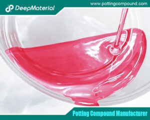
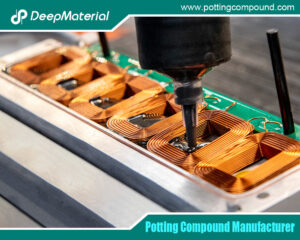
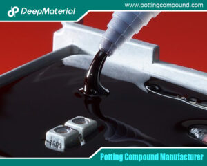
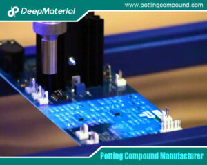
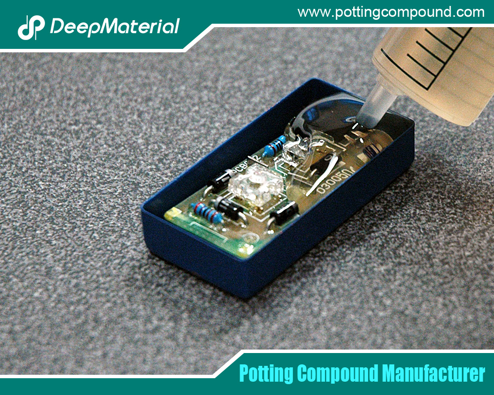
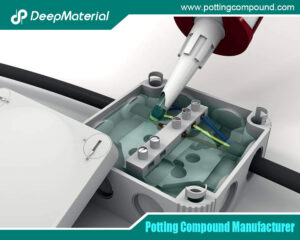
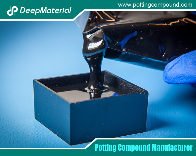
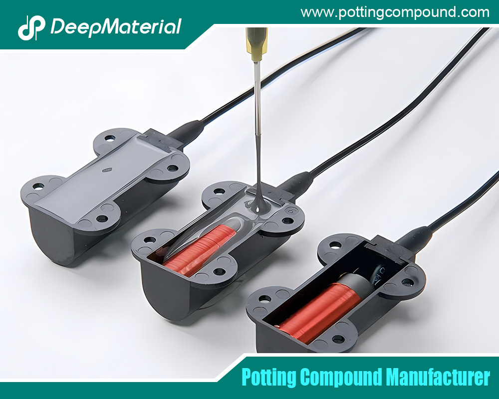
Encapsulation is the process of pouring the liquid encapsulation material into the PCB device with electronic components and circuits through mechanical or manual means. Under normal temperature or heating conditions, it will cure into a high-performance thermosetting polymer insulating material. After curing, the encapsulation material closely wraps the electronic components and circuits on the PCB, forming an integrated whole, just like putting a strong “armor” on the PCB. When the PCB is subjected to vibration and impact, the encapsulation material can disperse the stress, avoiding the concentration of stress at a certain point or area, thus protecting the PCB and components from damage.
(II) Commonly Used Encapsulation Materials
- Epoxy Resin Encapsulation Adhesive: It is mostly hard. After curing, it has a relatively high hardness, good mechanical strength, and electrical insulation performance. It has good adhesion to various metal and non-metal materials and can firmly adhere to the surface of the PCB. It has strong chemical corrosion resistance and can resist the erosion of a variety of chemical substances. The temperature resistance of ordinary epoxy resin encapsulation adhesive is about 100°C, and that of the heat-curing type can reach about 150°C. Some special formula products can withstand temperatures above 300°C. However, after curing, it is relatively brittle. When subjected to a large impact, it may crack itself, affecting the protection effect on the PCB. Moreover, it is difficult to remove after encapsulation, and the reworkability is poor.
- Silicone Encapsulation Adhesive: After curing, it is mostly soft and elastic, which makes it perform excellently in absorbing vibration and impact energy. Its adhesion is relatively poor, but it has strong anti-aging ability and good weather resistance, and can be used for a long time under harsh environmental conditions. It has excellent resistance to hot and cold changes and can maintain elasticity and not crack within the temperature range of -60°C to 200°C. Some heat-curing type products can withstand higher temperatures. It has good insulation performance, no corrosion to electronic components, and no by-products are generated during the curing reaction. In addition, the silicone encapsulation adhesive has excellent rework ability, and the sealed components can be conveniently and quickly taken out for repair and replacement.
- Polyurethane Encapsulation Adhesive: After curing, it is also soft and elastic, and its adhesion is between that of epoxy resin and silicone. It has the characteristics of low hardness, moderate strength, good elasticity, water resistance, and mildew prevention. It has excellent electrical insulation performance and flame retardancy, has no corrosion to electrical components, and has good adhesion to a variety of materials. However, its temperature resistance generally does not exceed 100°C, and bubbles are likely to occur during the encapsulation process. Usually, the encapsulation operation needs to be carried out under vacuum conditions.
The Specific Performance of Encapsulation in Improving the Seismic and Impact Resistance Performance of PCBs
(I) Enhancing Structural Integrity
After the encapsulation material cures, it closely combines all the components and circuits on the PCB together, forming a highly integrated overall structure. This integrity greatly enhances the anti-vibration and anti-impact ability of the PCB. Take the PCB in the engine control unit (ECU) of a car as an example. When the engine is running, strong vibrations will be generated. If the PCB is not encapsulated, the components may undergo relative displacement due to the vibrations, resulting in the loosening or even breaking of the solder joints. After encapsulation treatment, the encapsulation material fills the gaps between the components, firmly fixing them in their respective positions, effectively preventing displacement and damage caused by vibrations. When subjected to an impact, the encapsulation material can evenly disperse the impact force to the entire PCB, avoiding the damage to the components and circuits caused by local stress concentration.
(II) Dispersion of Stress
Vibrations and impacts will generate stress on the PCB, especially at the connection parts between components and the PCB and at the junctions of different materials, where the stress concentration phenomenon is more serious. The elasticity and flexibility of the encapsulation material enable it to effectively disperse these stresses. When the PCB is subjected to vibration, the encapsulation material can absorb the vibration energy through its own deformation and disperse the stress over a larger area, thereby reducing the stress value per unit area. For some surface-mounted devices (SMD), their solder joints with the PCB are prone to be affected by stress and crack under vibrations and impacts. The encapsulation material can form a buffer layer around the solder joints. When there is stress acting, the encapsulation material deforms first, dispersing the stress and reducing the stress borne by the solder joints, thus improving the reliability of the solder joints and reducing the risk of cracking.
(III) Protection of Solder Joints
Solder joints are the key parts of the electrical connection on the PCB and are also the parts most likely to have problems in a vibration and impact environment. Encapsulation has a direct protective effect on solder joints. On the one hand, the encapsulation material wraps the solder joints, providing physical protection for them and reducing the possibility of the solder joints being directly impacted. On the other hand, as mentioned before, the encapsulation material can disperse the stress and reduce the force on the solder joints during vibrations and impacts. In an experiment on a mobile phone motherboard, the motherboard without encapsulation and the encapsulated motherboard were tested for vibration. The results showed that a large number of solder joints on the unencapsulated motherboard cracked after a certain period of vibration, while almost no problems occurred with the solder joints on the encapsulated motherboard. This fully demonstrates the effectiveness of encapsulation in protecting solder joints.
(IV) Reducing the Influence of Resonance
In a vibration environment, the PCB has a natural frequency. When the external vibration frequency is close to the natural frequency of the PCB, a resonance phenomenon will occur. Resonance will cause the vibration amplitude of the PCB to increase sharply, thus causing serious damage to the components and circuits on it. The addition of the encapsulation material changes the mass distribution and stiffness of the PCB, thereby changing its natural frequency, making the natural frequency of the PCB错开 from the possible external vibration frequencies and avoiding the occurrence of resonance. For example, in the PCB of the controller of an industrial robot, through the encapsulation treatment, the natural frequency of the PCB is effectively adjusted, so that it will not resonate due to the vibrations of components such as motors during the operation of the robot, ensuring the stable operation of the controller.
Quantitative Analysis of the Performance Improvement by Encapsulation
To more intuitively understand the degree of improvement of the seismic and impact resistance performance of PCBs by encapsulation, let’s look at some actual test data and cases. In the laboratory environment, the vibration tests were carried out on the same type of PCB before and after encapsulation respectively. The test equipment used is a vibration table to simulate different vibration frequencies and accelerations. The results showed that for the unencapsulated PCB, when the vibration acceleration reached 5g, the fracture of component pins and the cracking of solder joints began to occur; while for the same PCB after encapsulation treatment, when the vibration acceleration reached 15g, it could still work normally, and no obvious damage occurred to the components and solder joints. This indicates that the encapsulation has increased the seismic resistance of the PCB by at least 3 times.
In the field of automotive electronics, an automobile manufacturer made encapsulation improvements to the PCB of its in-vehicle entertainment system. In the actual road test, the failure rate of the unencapsulated PCB due to vibrations and impacts after a certain period of driving was 10%; after adopting the encapsulation process, the failure rate was reduced to less than 1%. This significant data comparison fully reflects the great role of encapsulation in improving the anti-vibration and anti-impact performance of PCBs and thus enhancing the reliability of products.
Encapsulation Process and Precautions
(I) Encapsulation Process
Common encapsulation processes include manual encapsulation and mechanical encapsulation. Manual encapsulation is simple to operate and has a low cost, but its efficiency is not high, and the encapsulation quality is greatly affected by the technical level and proficiency of the operator, making it difficult to ensure consistency. Mechanical encapsulation, with the help of automated equipment, can achieve accurate measurement and uniform pouring, with high efficiency and stable quality, and is suitable for large-scale production. In mechanical encapsulation, it can be further divided into vacuum encapsulation and non-vacuum encapsulation. Vacuum encapsulation can remove the bubbles in the encapsulation material, improve the compactness and reliability of the encapsulation, and is especially suitable for occasions with high requirements for airtightness and electrical performance; non-vacuum encapsulation is relatively simple and has a lower cost, but there may be some bubbles remaining in the encapsulation material.
(II) Precautions
- Preparatory Work Before Encapsulation: It is necessary to ensure that the surface of the PCB is clean, free of dust, oil stains, and other impurities. Otherwise, it will affect the adhesion effect between the encapsulation material and the PCB. For some sensitive components, appropriate protection may be required to avoid damage to them by the encapsulation material.
- Selection of Encapsulation Material: The appropriate encapsulation material should be selected according to the specific application scenarios and requirements. As described before, different encapsulation materials have their own advantages and disadvantages in performance. Factors such as temperature resistance, seismic resistance, waterproof performance, electrical performance, and rework requirements need to be comprehensively considered.
- Control of the Encapsulation Process: Strictly control the parameters such as the proportioning, mixing uniformity, pouring speed, and temperature of the encapsulation material. If the proportioning is inaccurate, it may lead to incomplete curing of the encapsulation material or a decline in its performance; uneven mixing will cause local differences in the performance of the encapsulation material; too fast a pouring speed is likely to generate bubbles, and too slow a speed will affect the production efficiency; inappropriate temperature will affect the fluidity and curing time of the encapsulation material.
- Curing Conditions: Provide appropriate curing temperature and time according to the requirements of the encapsulation material. Incomplete curing will prevent the encapsulation material from achieving the expected performance and affect the protection effect on the PCB.
Conclusion
Encapsulation has a remarkable effect in improving the seismic and impact resistance performance of PCBs. Through multiple ways such as enhancing structural integrity, dispersing stress, protecting solder joints, and reducing the influence of resonance, it provides a powerful guarantee for the stable operation of PCBs in complex vibration and impact environments. In practical applications, reasonably selecting the encapsulation material and process and strictly controlling each link can give full play to the advantages of encapsulation, improving the reliability and service life of electronic devices. With the continuous development of electronic technology, the encapsulation technology will also continue to innovate and improve to meet the growing demand for high-performance electronic devices.
For more about analysis of the improvement of the seismic and impact resistance performance of PCB by encapsulation, you can pay a visit to DeepMaterial at https://www.pottingcompound.com/ for more info.