Phone: +86-133 5263 6504
Phone: +86-133 5263 6504

How to Prevent Voids in Circuit Board Potting: A Comprehensive Guide to Reliable Encapsulation
Potting, the process of encapsulating a printed circuit board (PCB) potting assembly in a protective resin, is a critical step in the manufacture of robust electronics. It provides superior defense against mechanical shock, vibration, moisture, dust, chemicals, and thermal stress. However, the integrity and protective qualities of a potted assembly can be catastrophically compromised by one common flaw: voids.
Voids are air pockets or unfilled cavities trapped within the cured potting material. These defects act as insulating hotspots, reduce dielectric strength, create pathways for moisture ingress, induce mechanical stress concentrations, and hinder thermal dissipation—any of which can lead to premature device failure in the field. Preventing voids is not merely a cosmetic concern; it is a fundamental requirement for reliability.
This article provides a systematic, technical deep-dive into the root causes of void formation and outlines a comprehensive strategy for their prevention, covering material selection, process engineering, and design considerations.
Understanding the Enemy: The Root Causes of Voids
To prevent voids, one must first understand how they are born. Voids originate from three primary sources:
- Entrapped Air: Air physically trapped during the mixing or pouring process around complex components, under components, or within cavities of the housing.
- Outgassing: The release of volatile substances (moisture, solvents, air) from the PCB substrate, components, conformal coatings, or even the potting material itself during the curing exotherm.
- Shrinkage Voids: Localized cavities formed when the potting compound undergoes volumetric shrinkage during cure, especially if it occurs after the material has gelled and can no longer flow to compensate.
The prevention strategy is a multi-front battle against these causes.
The Foundation: Material Selection and Preparation
The journey to a void-free pot begins long before the resin is poured.
- Choosing the Right Potting Compound:
Not all resins behave alike. Key properties to scrutinize include:
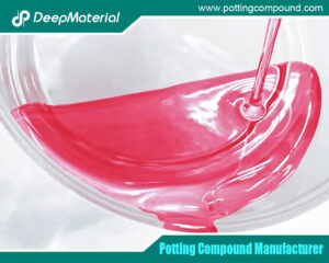
- Viscosity & Flow: Low-viscosity resins (e.g., many epoxies and silicones) flow more easily, wetting components and penetrating tight spaces to displace air. However, too low a viscosity can lead to leakage. Thixotropic materials that shear-thin during pouring are often ideal.
- Pot Life & Gel Time: A sufficiently long pot life allows air bubbles time to rise to the surface before gelation. Conversely, an excessively long open time can allow settled fillers to separate.
- Cure Profile & Shrinkage: Materials with a low coefficient of thermal expansion (CTE) and minimal cure shrinkage (e.g., silicones, flexible epoxies) are less prone to pulling away from components or creating internal shrinkage voids. A slow, controlled cure generates less exothermic heat, reducing outgassing.
- Degassing Properties: Some formulated systems are inherently better at releasing entrapped air.
- Critical Pre-Potting Preparation: Baking (Pre-Drying)
This is arguably the single most important step for preventing outgassing voids.
- Why: PCBs, components, and plastic housings are hygroscopic. Absorbed moisture vaporizes rapidly during the potting cure, creating bubbles that become trapped.
- How: Bake assemblies in a controlled oven. A typical regimen is 2-4 hours at 80-125°C, depending on the thermal sensitivity of components. Ensure the baking temperature exceeds the maximum expected temperature during the potting exotherm.
- Handling: Post-baking, assemblies must be potted immediately or stored in a dry, climate-controlled environment. Use desiccated storage cabinets if a delay is unavoidable.
Surface Priming and Wettability
For some materials (especially non-polar substrates like polyamide housings or certain conformal coatings), applying a compatible primer or adhesion promoter can dramatically improve resin wettability. This helps the potting material flow across surfaces, rather than pulling away and creating voids at interfaces.
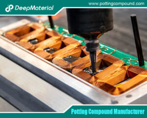
A. The Process: Engineering the Pour for Perfection
The execution of the circuit board potting process is where theory meets practice.
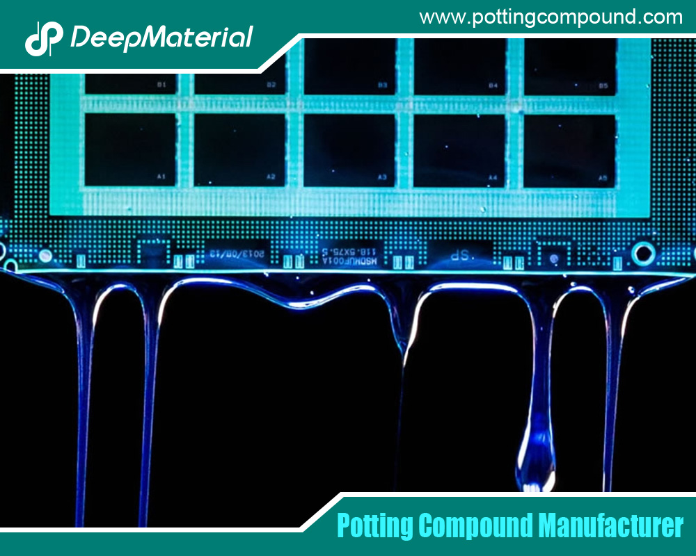
- Mixing Methodology: The Birthplace of Bubbles
- Manual vs. Mechanical: Always use a controlled mechanical mixing system (dual-cartridge dispensers or meter-mix-dispense (MMD) equipment) over manual mixing. Manual stirring aggressively incorporates air.
- Vacuum Degassing of Mixed Resin: For critical applications, the mixed resin can be placed in a vacuum chamber before dispensing. Applying a vacuum (typically 25-29 in. Hg) for several minutes expands and collapses entrapped air bubbles in the liquid. This pre-degassing step is highly effective.
- Slow and Deliberate: Even with mechanical mixing, use the slowest speed that achieves homogeneous blending. Mixing blades should be designed to fold material, not whip it.
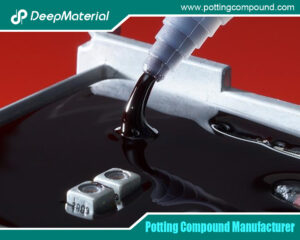
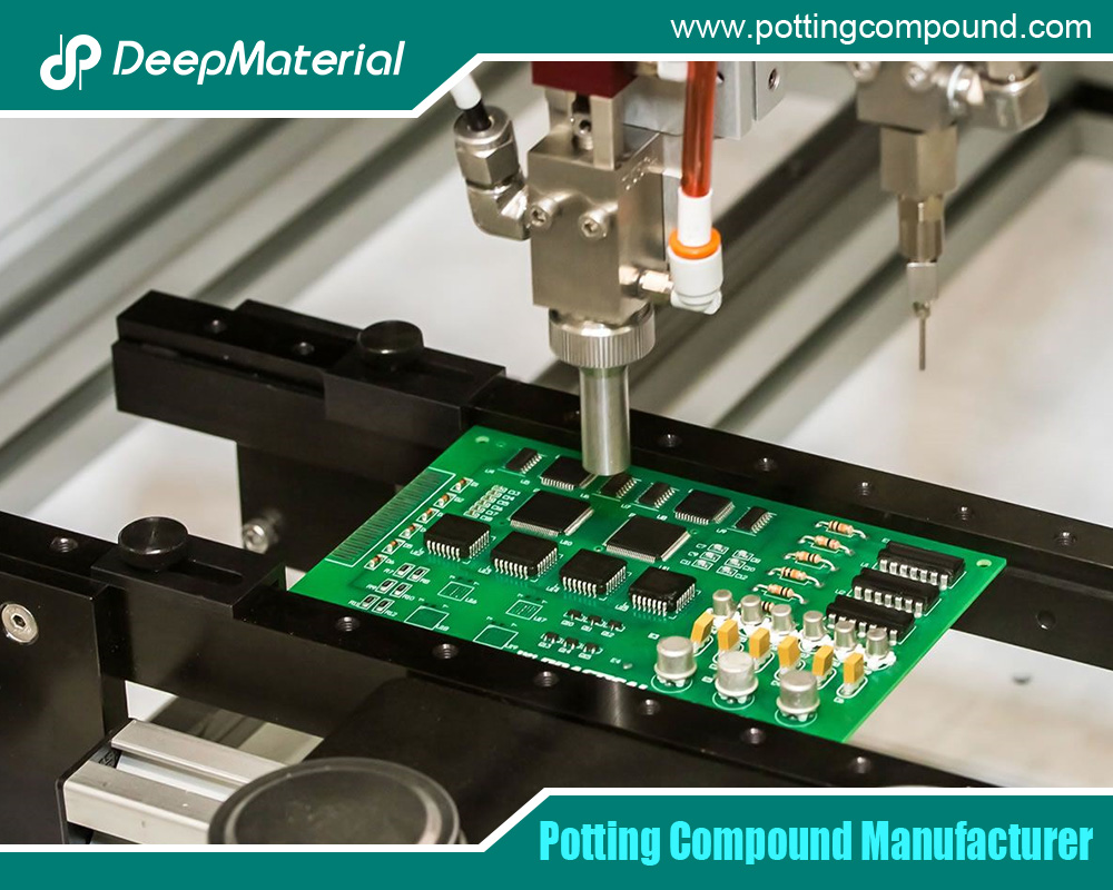
B. Dispensing Technique: The Art of Controlled Flow
- Dispense Path: Pour or dispense the resin in a slow, steady stream at the lowest point of the cavity, allowing it to rise evenly and progressively. Never pour directly onto components or from a great height, which traps air. Use a nozzle to direct the flow along the side of the housing.
- Angle of Pour: Tilt the assembly slightly to encourage material to flow up one side, allowing air to escape from the opposite side—a technique akin to soldering.
- Multiple Stages: For deep fills or extremely dense assemblies, consider a two-stage potting process. A first, thin “encapsulation” layer can wick around components. After a partial gel, a second fill layer completes the process, reducing the total hydrostatic pressure and outgassing path length.
C. The Ultimate Tool: In-Situ Vacuum Potting
For the highest reliability standards, in-situ vacuum potting is the gold standard.
- The prepared assembly is placed in a vacuum chamber.
- The resin is dispensed onto the assembly under vacuum. With ambient pressure drastically reduced, any air present expands and is evacuated from the resin and assembly surfaces instantly.
- After dispensing, atmospheric pressure is gradually restored. This 14.7 psi pressure forcefully drives the resin into every micron-scale crevice, resulting in a near-perfect, void-free encapsulation. This process effectively eliminates both entrapped air and outgassing voids.
D. Curing Cycle: Patience is a Virtue
- Controlled Ramp: If post-cure heating is required, use a gradual temperature ramp (e.g., 2-5°C per minute). A sudden temperature spike can cause rapid outgassing.
- Gel Before Full Cure: Allow the material to gel at room temperature before applying heat. This ensures it has sufficient structural strength to hold bubbles in place, preventing them from rising and creating large voids at the top.
The Supporting Role: PCB and Enclosure Design
Prevention starts at the drawing board. Design For Manufacturing (DFM) for potting is essential.
- Component Layout and Spacing: Avoid creating “bathtub” configurations where large components (e.g., tall capacitors, connectors) are surrounded by walls of smaller parts. These trap air. Stagger component heights where possible and provide clear channels for resin flow from the pour point to all areas.
- Venting and Fill Ports: Design the enclosure with strategically placed vent holes opposite the fill port. This allows displaced air a clear escape route. The vent should be sized to avoid resin bleed but permit air passage. Consider using porous vents or gels.
- Sharp Edges and Corners: Radius internal corners of the potting dam or enclosure. Sharp 90-degree corners are notorious for trapping air bubbles.
- Under-Component Clearance: Specify a minimum standoff height for large components (like QFPs or BGAs) if possible. Even a 0.5mm gap allows resin to flow underneath, preventing a large void that can also act as a moisture reservoir.
- Material Compatibility: Ensure all materials in the assembly (PCB laminate, solder mask, component bodies, adhesives, housing) are compatible with the potting compound’s chemistry and cure temperature to prevent delamination or chemical outgassing.
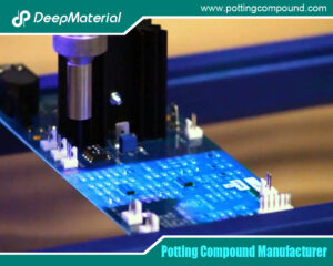
Verification and Quality Control
You cannot control what you do not measure. Implement QC checks to catch process drift.
- Visual Inspection (Post-Cure): Use bright, angled lighting to inspect for surface voids or sink marks indicating subsurface issues.
- Non-Destructive Testing (NDT):
- Ulasonic Scanning (C-Scan): The most common method. High-frequency sound waves reflect off voids, creating a map of their size and location within the potted module.
- X-Ray Inspection: Effective for locating voids, especially in areas with metal shielding or high-density components that may challenge ultrasonic methods.
- Destructive Analysis: For process validation or failure analysis, cross-sectioning a sample potted unit provides undeniable evidence of void presence, location, and root cause (e.g., outgassing from a specific component).
Conclusion:
Preventing voids in circuit board potting is not a matter of a single “silver bullet.” It is the result of a holistic, disciplined system that integrates:
- Informed Material Science: Selecting a resin system with appropriate flow, cure, and degassing properties.
- Meticulous Preparation: Rigorously baking assemblies to eliminate moisture.
- Precision Process Engineering: Employing degassing, controlled dispensing, and ideally, vacuum potting technology.
- Proactive Design: Designing the PCB and enclosure to facilitate, not hinder, the potting process.
By treating potting not as a simple “pour-and-go” operation but as a critical, controllable chemical and mechanical process, engineers can consistently achieve void-free encapsulations. This diligence pays direct dividends in the form of enhanced product reliability, longer service life, and the prevention of costly field failures—securing the protective fortress that potting is intended to be.
For more about how to prevent voids in circuit board potting: a comprehensive guide to reliable encapsulation, you can pay a visit to DeepMaterial at https://www.pottingcompound.com/ for more info.