Phone: +86-133 5263 6504
Phone: +86-133 5263 6504
A Comprehensive Analysis of the Compatibility between Encapsulation Materials and PCBs: Exploration of Chemical Reactions and Their Impact on Performance
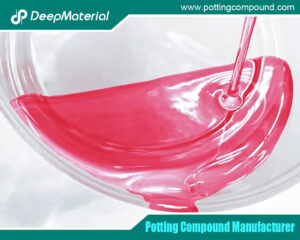
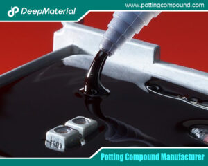
In the field of electronic device manufacturing, the use of encapsulation materials is crucial for protecting the electronic components on printed circuit boards (PCBs) and enhancing the stability of the devices. Encapsulation materials can not only provide protection against water, dust, and shock but also improve the electrical insulation performance. However, the compatibility issue between the encapsulation materials and various components, coatings, as well as substrate materials on the PCB is a key factor in ensuring the long-term stable operation of electronic products. Once a chemical reaction occurs, it may lead to a decline in performance and even cause equipment failures. This article will delve into the compatibility between the encapsulation materials and each component of the PCB, analyze the possibility of chemical reactions, and explore their impact on performance.
Compatibility between Encapsulation Materials and Components
(A) Metal Components
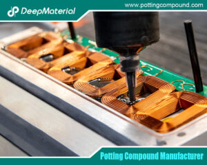
There are a large number of metal components on the PCB, such as pins and soldering points. Certain components in the encapsulation materials may react chemically with the metals, leading to corrosion or oxidation. Take epoxy resin encapsulation materials as an example. If acidic substances are generated during the curing process, they may react with copper pins, forming copper salts. This will damage the electrical conductivity and mechanical strength of the metal, affecting the electrical connection between the component and the PCB. In severe cases, it may lead to open circuit failures. When selecting encapsulation materials, their chemical properties need to be considered, and materials that may have adverse reactions with metals should be avoided. Some encapsulation materials with special formulations can form a protective film on the metal surface, reducing the occurrence of chemical reactions.
(B) Semiconductor Components
Semiconductor components are quite sensitive to environmental changes, and the compatibility between the encapsulation materials and semiconductor components directly affects their performance. Silicone encapsulation materials usually have good chemical stability and low stress characteristics, having relatively little impact on semiconductor components. However, if the encapsulation materials contain impurities or small molecular substances, they may penetrate into the interior of the semiconductor components, changing their electrical properties and resulting in parameter drift or failure. For example, some low-quality encapsulation materials may release sulfur-containing compounds under high-temperature environments, reacting with the metal electrodes in the semiconductor components to form sulfides, increasing the contact resistance and affecting the normal operation of the components. To ensure the stable performance of semiconductor components, encapsulation materials with high purity and good compatibility should be selected, and appropriate pretreatment, such as cleaning and drying, should be carried out on the components before encapsulation.
Compatibility between Encapsulation Materials and PCB Coatings
(A) Three-proof Paint Coatings
Three-proof paint is a common PCB coating used to protect the circuit board from moisture, dust, and chemical substances. When the encapsulation materials come into contact with the three-proof paint coatings, chemical reactions may occur, affecting the protective effects of both. If the solvents in the encapsulation materials are not compatible with the three-proof paint, it may cause the three-proof paint to dissolve or swell, damaging its integrity and reducing the protective performance. In addition, the stress generated during the curing process of the encapsulation materials may also cause the three-proof paint coating to crack. In practical applications, compatibility tests need to be carried out, and encapsulation materials that are compatible with the three-proof paint should be selected. A small area of the PCB sample can be used for encapsulation and coating tests first, and observe whether there are adverse reactions, such as color changes, blistering, or peeling.
(B) Solder Mask Layer
The solder mask layer is an important coating on the PCB, used to prevent solder bridging and short circuits. The compatibility issue between the encapsulation materials and the solder mask layer mainly lies in adhesion and chemical stability. If the adhesion between the encapsulation materials and the solder mask layer is insufficient, delamination may occur when subjected to vibration or temperature changes, affecting the encapsulation effect. In addition, certain encapsulation materials may react chemically with the organic components in the solder mask layer, causing the solder mask layer to discolor and become brittle. To improve the compatibility between the encapsulation materials and the solder mask layer, encapsulation materials with good adhesion can be selected, and surface treatment, such as sanding and cleaning, can be carried out on the PCB before encapsulation to enhance the bonding force between them.
Compatibility between Encapsulation Materials and Substrate Materials
(A) Common Substrate Materials
There are various types of PCB substrate materials, and common ones include FR-4 (glass fiber reinforced epoxy resin), CEM-1 (composite epoxy resin), polyimide, etc. Different substrate materials have different chemical structures and physical properties, and their compatibility with encapsulation materials also varies. The FR-4 substrate is one of the most widely used ones, which has good mechanical and electrical properties. However, the epoxy resin components in the FR-4 substrate may react chemically with certain encapsulation materials, especially in high-temperature and high-humidity environments, where the reaction rate may increase. Therefore, when selecting encapsulation materials, the characteristics of the substrate materials need to be considered to avoid a decline in the performance of the substrate due to chemical reactions.
(B) Impact of Chemical Reactions on Substrate Performance
The chemical reaction between the encapsulation materials and the substrate materials may cause a change in the expansion coefficient of the substrate, resulting in thermal stress when the temperature changes, and triggering substrate deformation and cracking. Such deformation and cracking will not only affect the mechanical strength of the PCB but also may lead to the cracking of component solder joints, causing electrical failures. In addition, chemical reactions may also reduce the insulation performance of the substrate, increasing the risk of leakage. For example, when the acidic substances in the encapsulation materials react with the alkaline components in the substrate, conductive substances may be generated, reducing the insulation resistance of the substrate. To evaluate the compatibility between the encapsulation materials and the substrate materials, tests such as thermomechanical analysis (TMA) and dynamic mechanical analysis (DMA) can be carried out to monitor the performance changes of the substrate before and after encapsulation.
Compatibility Test Methods and Evaluation Criteria
(A) Laboratory Test Methods
- Accelerated Aging Test: By simulating harsh environmental conditions such as high temperature, high humidity, and thermal cycling, the chemical reactions between the encapsulation materials and each component of the PCB are accelerated, and their compatibility can be evaluated in a relatively short period. For example, place the encapsulated PCB sample in a high-temperature and high-humidity test chamber, and keep it under certain temperature and humidity conditions for a period of time, and then observe whether the sample has phenomena such as corrosion, discoloration, and delamination.
- Infrared Spectroscopy Analysis: Use an infrared spectrometer to analyze the materials before and after encapsulation, detect the changes in chemical bonds, and determine whether a chemical reaction has occurred. By comparing the infrared spectra of the materials before and after encapsulation, new absorption peaks or changes in the intensity of absorption peaks can be found, so as to determine the occurrence of chemical reactions and the reaction products.
- Scanning Electron Microscope (SEM) Observation: Use SEM to observe the microscopic structure of the interfaces between the encapsulation materials and each part of the PCB, check for defects such as cracks, voids, and corrosion marks, and evaluate the bonding situation and compatibility of the interfaces. SEM can provide high-resolution images, helping analysts more intuitively understand the microscopic state of the material interfaces.
(B) Industry Evaluation Criteria
At present, the electronics industry has formulated a series of evaluation criteria for the compatibility between encapsulation materials and PCBs, such as the IPC-TM-650 series of test methods. These criteria cover test requirements in multiple aspects such as physical properties, chemical properties, and electrical properties, providing an important basis for the selection and application of encapsulation materials. In actual production, enterprises should refer to relevant standards for compatibility tests and evaluations according to the usage environment and performance requirements of the products to ensure the quality and reliability of the products.
The compatibility between the encapsulation materials and various components, coatings, and substrate materials on the PCB is a complex and crucial issue. By deeply understanding the possible chemical reactions and their impact on performance, adopting scientific test methods and evaluation criteria, selecting appropriate encapsulation materials, and strictly controlling the process parameters during production, the compatibility between the encapsulation materials and the PCB can be effectively improved, ensuring the long-term stable operation of electronic products. In the future manufacturing of electronic devices, with the continuous emergence of new materials and new processes, the compatibility issue will continue to receive attention, and the industry needs to continuously explore and study new solutions.
For more about choosing a comprehensive analysis of the compatibility between encapsulation materials and PCBs: exploration of chemical reactions and their impact on performance, you can pay a visit to DeepMaterial at https://www.pottingcompound.com/ for more info.