Phone: +86-133 5263 6504
Phone: +86-133 5263 6504
A Comprehensive Analysis of Post-Potting PCB Issues and the Repair and Rework of Potting Materials
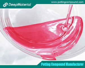
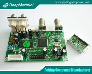
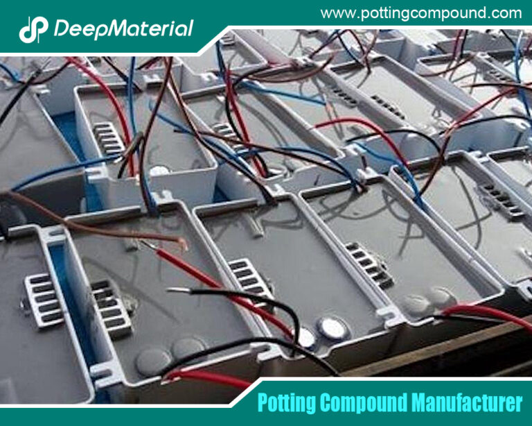
In the field of electronic manufacturing, PCB (Printed Circuit Board) potting is a crucial process. It can provide protection for electronic components, shielding them from moisture, dust, chemicals, and mechanical stress. This significantly enhances the reliability and stability of electronic products. However, even with strict control over the production process, post-potted PCBs may still encounter various problems. When these issues occur, the repair or rework of the potting materials becomes a challenging but necessary task.
Common Problems of Post-Potted PCBs and Cause Analysis
Electrical Performance Failures
- Short Circuit: Conductive impurities may be mixed into the potting material. These impurities may move to unintended positions during or after the potting process, creating unexpected conductive paths between different circuits. Additionally, if conductive residues such as solder balls on the PCB are not thoroughly cleaned before potting, they may also cause short circuits after potting.
- Open Circuit: The potting material may generate shrinkage stress during the curing process. If this stress acts on the pins of electronic components or the circuits of the PCB, it may lead to pin breakage or circuit cracking, resulting in an open circuit. Moreover, drastic temperature changes may cause a significant difference in the coefficient of thermal expansion between the potting material and the electronic components or the PCB, which can also trigger similar problems.
- Decrease in Insulation Performance: The insulation performance of the potting material may gradually decline if it is exposed to harsh environments such as high temperature and high humidity for a long time. For example, in some outdoor electronic products, the potting material is exposed to sunlight and humid air for an extended period, making it prone to such issues. In addition, quality problems of the potting material itself or incomplete curing can also lead to the insulation performance failing to meet the expected standards.
Potting Material-Related Issues
- Cracking of the Potting Material: This may be due to the insufficient flexibility of the potting material. When subjected to external forces such as temperature changes and mechanical vibrations, it cannot effectively buffer the stress, resulting in cracking. At the same time, too fast a curing speed in the potting process can cause stress concentration inside the potting material, which is also likely to lead to cracking.
- Debonding of the Potting Material from the PCB or Components: Inadequate cleaning of the surface of the PCB or components before potting, leaving residues such as oil stains and dust, will affect the adhesion between the potting material and them. In addition, the mismatch between the potting material and the materials of the PCB or components may also result in insufficient bonding force, leading to debonding problems.
- Residual Bubbles in the Potting Material: During the potting process, if the potting material is not properly stirred, excessive bubbles will be introduced. Moreover, if effective defoaming measures, such as vacuum degassing, are not taken during potting, these bubbles will remain inside the potting material. The presence of bubbles not only affects the mechanical properties of the potting material but also may reduce its electrical insulation performance.
Component Damage
- Overheating Damage: Electronic components generate heat during operation. If the thermal conductivity of the potting material is poor, the heat cannot be dissipated in a timely manner, causing the temperature of the components to be too high and eventually leading to damage. In addition, an unreasonable heat dissipation design, such as poor contact between the heat sink and the components, will exacerbate this situation.
- Mechanical Stress Damage: When the post-potted PCB is subjected to mechanical external forces such as bumps during transportation or improper operation during installation, the potting material may transmit these stresses to the components, causing damage to the internal structure of the components. For example, if excessive pressure is applied to the PCB during installation, it may cause the pins of the components to break or the internal chips to be damaged.
Preparation Work before the Repair or Rework of Potting Materials
Preparation of Tools and Equipment
- Heating Equipment: Such as hot air guns and heating tables, are used to heat the potting material to soften it for removal. A hot air gun can provide local high temperature and is suitable for removing the potting material around small components. A heating table can evenly heat the entire PCB and is more suitable for the treatment of large-area potting materials.
- Removal Tools: Including tweezers, scrapers, and needle-nose pliers. Tweezers can be used to carefully pick up components or remove small pieces of potting material. Scrapers can be used to scrape off the cured potting material. Needle-nose pliers can be used to cut component pins or remove larger pieces of potting material.
- Cleaning Tools and Reagents: Cleaning agents such as anhydrous alcohol and isopropyl alcohol, as well as cleaning tools such as soft brushes and cotton swabs. Anhydrous alcohol and isopropyl alcohol have good solubility and volatility and can effectively remove residual potting materials, soldering fluxes, and other impurities on the PCB. Soft brushes and cotton swabs are used for fine cleaning operations to avoid scratching the surface of the PCB.
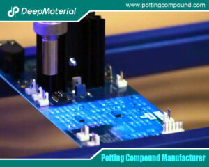
- Testing Equipment: Electrical performance testing equipment such as multimeters and oscilloscopes, as well as microscopes and other equipment for observing the surface conditions of the PCB and components. A multimeter can be used to detect the continuity of circuits and resistance values. An oscilloscope can analyze signals to help determine whether the electrical performance is normal. A microscope can magnify the details of the surface of the PCB and components, making it easy to detect small cracks, debonding, and other problems.
Safety Protection Measures
- Wear Protective Equipment: Operators should wear protective glasses to prevent debris of the potting material or other foreign objects from entering the eyes during the removal of the potting material. At the same time, gloves should be worn to avoid direct contact between the skin and the potting material and cleaning agents, as some potting materials and cleaning agents may be irritating or corrosive to the skin. In addition, masks should be worn to prevent the inhalation of harmful gases generated when heating the potting material.
- Ensure Good Ventilation in the Working Environment: The potting material will release harmful gases, such as volatile organic compounds (VOCs), during the heating process. Therefore, the operation should be carried out in a fume hood or an environment with good ventilation equipment to ensure that the air breathed by the operators is clean and safe.
Evaluate the Feasibility of Repair or Rework
- Analyze the Severity of the Problem: Through testing equipment and observation, comprehensively evaluate the damage situation of the PCB and components. If there are only slight cracks on the surface of the potting material or a small area of debonding, and the electrical performance is not affected, the repair is relatively simple. However, if there are serious short circuits, open circuits, or a large number of damaged components, the difficulty and cost of repair will increase significantly, and it may even be necessary to consider remaking the PCB.
- Consider Cost and Time Factors: Repair or rework requires the investment of human, material, and time costs. For some low-value PCBs or products, if the repair cost is too high or takes too long, it may be more cost-effective to directly replace the PCB with a new one. For some high-end, customized PCBs that are difficult to replace quickly, even if the repair is difficult, efforts should be made to repair them. At the same time, it is also necessary to consider whether the repaired PCB can meet the remaining service life and performance requirements of the product.
Specific Methods for the Repair or Rework of Potting Materials
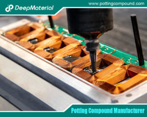
Heating and Softening Removal Method
- For Epoxy Resin Potting Materials: Epoxy resin potting materials are relatively hard after curing and usually require a high temperature to soften. When using a hot air gun, the temperature can be set at about 300 – 400°C, and the airspeed can be adjusted according to the actual situation, generally maintaining a moderate level to avoid blowing off surrounding components with excessive wind force. Keep the hot air gun about 3 – 5 cm away from the surface of the potting material and move the hot air gun evenly to make the potting material heat evenly and gradually soften. When the potting material is softened to a certain extent, carefully remove it with a scraper or tweezers. During the removal process, pay attention to avoid scratching the circuits and components on the surface of the PCB.
- For Silicone Potting Materials: Silicone potting materials are more flexible than epoxy resin potting materials and have a relatively lower softening temperature. When using a hot air gun, the temperature can be set at about 200 – 300°C, and maintain an appropriate airspeed and distance for heating. After the potting material is softened, peel it off with tools. For some parts that adhere tightly to the components or the PCB, solvents (such as acetone, etc., but pay attention to the impact of the solvent on the PCB and components) can be used for infiltration first, and then removed, which can reduce the damage to the components and the PCB.
Solvent Dissolution Method
- Applicable Solvents and Precautions: For silicone potting materials, solvents such as acetone and toluene have better dissolution effects; for epoxy resin potting materials, some special epoxy resin dissolvents may be more effective. When using solvents, it is necessary to ensure that the solvents will not cause damage to the components, circuits, and other materials on the PCB. For example, some solvents may dissolve the solder mask layer on the surface of the PCB or corrode the casings of electronic components. Therefore, before use, a small-scale test should be carried out on an inconspicuous part of the PCB. After observing for a period of time, if there are no adverse reactions, then use it on a large area.
- Specific Operation Steps: Drop an appropriate amount of solvent on the surface of the potting material and let the solvent fully penetrate into the potting material. Depending on the thickness and curing degree of the potting material, wait for a few minutes to dozens of minutes to make the potting material fully dissolve or swell. Then, gently wipe with a soft brush or cotton swab to remove the dissolved potting material. For some remaining parts that are difficult to wipe clean, solvent can be repeatedly dropped and wiped until the potting material is completely removed. During the operation, pay attention to ventilation to avoid the harm caused by the gas volatilized from the solvent to the human body.
Mechanical Removal Method
- Use of Tools and Operation Key Points: When the potting material is thin and does not adhere particularly tightly to the components or the PCB, tools such as tweezers and scrapers can be directly used for mechanical removal. When using tweezers, carefully clamp the edge of the potting material and gently lift it up, avoiding excessive force that may damage the components or circuits. The scraper should be sharp and made of hard material, such as a stainless steel scraper. Place the edge of the scraper close to the interface between the potting material and the PCB or components and gently scrape off the potting material at a certain angle. During the scraping process, pay attention to controlling the force and angle to avoid scratching the surface of the PCB.
- Treatment Methods for Different Situations: If the potting material covers the pins of the components, be especially careful when removing it to avoid damaging the pins. You can first use needle-nose pliers to carefully crush the potting material around the pins and then gradually remove it. For some large-area potting materials, they can be divided into small pieces first and then removed separately, which can reduce the difficulty of removal and minimize the damage to the PCB and components.
The Process of Repotting
- Clean the Surface of the PCB: After removing the old potting material, thoroughly clean the surface of the PCB with anhydrous alcohol or isopropyl alcohol to remove residual potting materials, soldering fluxes, and impurities. You can dip a soft brush in the cleaning agent and gently scrub the surface of the PCB, especially the pins of the components, circuits, and other parts, to ensure that the surface is clean and free of contamination. Then, dry the surface of the PCB with a clean cotton swab or paper towel, or use a hot air gun to dry it at a low temperature. Note that the temperature should not be too high to avoid damaging the components.
- Inspect the Components and Circuits: Carefully check whether the components are damaged, whether the pins are broken, and whether the circuits are cracked through a microscope. For the discovered problems, repair them in a timely manner. For example, if the pins of the components are broken, they can be repaired by soldering with a soldering iron and solder; if the circuits are cracked, methods such as flying wires can be used for connection. At the same time, use testing equipment such as a multimeter to conduct a preliminary test on the electrical performance of the PCB to ensure that there are no short circuits, open circuits, and other problems.
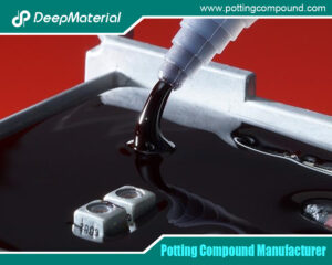
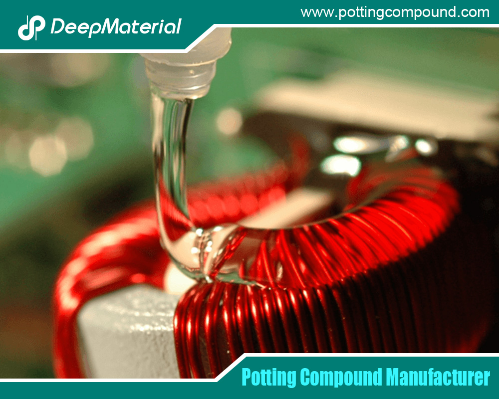
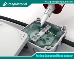
- Select the Appropriate Potting Material and Potting Process: Select the appropriate potting material according to the operating environment of the PCB, electrical performance requirements, and the characteristics of the components. For example, for PCBs used in high-temperature environments, potting materials with good high-temperature resistance should be selected; for occasions with high requirements for electrical insulation performance, potting materials with excellent insulation performance should be chosen. In terms of the potting process, if high precision of potting is required, an automatic dispensing device can be used; for small PCBs or a small number of potting requirements, manual potting is also a feasible method. Before potting, according to the instructions of the potting material, fully stir and mix the potting material (if it is a two-component potting material), and pay attention to removing bubbles.
- Potting and Curing: Slowly pour the prepared potting material onto the PCB to ensure that the potting material evenly covers the components and circuits that need to be protected, and avoid problems such as missed potting and bubbles. For potting processes that are prone to generating bubbles, a vacuum potting method can be adopted, that is, potting in a vacuum environment to reduce the generation of bubbles. After potting is completed, carry out the curing treatment according to the curing conditions of the potting material. If it is a room-temperature curing potting material, place the PCB in a well-ventilated and suitable temperature environment for natural curing; if it is a heat-curing potting material, put the PCB into an oven or heating equipment and carry out heat curing according to the specified temperature and time. During the curing process, avoid the PCB from being vibrated or disturbed by external forces to avoid affecting the potting effect.
Inspection and Verification after Repair or Rework
Appearance Inspection
- Check the Integrity of the Potting Material: Observe whether the surface of the repotted potting material is flat and smooth, and whether there are defects such as cracks, bubbles, and holes. The potting material should completely cover the components and circuits that need to be protected, and the edges should be neat without phenomena such as flowing and piling up.
- Confirm that the Components and Circuits are Undamaged: Carefully check whether the pins of the components are normally connected, whether there are deformations, breakages, and other situations through a microscope; whether the circuits are clear, and whether there are problems such as short circuits, open circuits, and scratches. At the same time, check whether the positions of the components are correct and whether there are any offsets or looseness.
Electrical Performance Testing
- Use Professional Equipment for Testing: Use a multimeter to test the resistance value and continuity of the circuits to ensure that the resistance value is within the normal range and there are no open circuit phenomena. Use an oscilloscope to test the signal transmission situation and observe whether the waveform of the signal is normal and whether there are problems such as distortion and interference. For some PCBs with high requirements for electrical performance, it may also be necessary to use an insulation resistance tester to test the insulation resistance and a withstand voltage tester to test the withstand voltage performance.
- Simulate the Actual Working Environment for Testing: In order to more comprehensively verify the performance of the repaired or reworked PCB, install it into the actual equipment and conduct tests in an environment that simulates the actual working conditions. For example, for PCBs that work in a high-temperature environment, put the equipment into a high-temperature chamber and run it for a period of time under the set high-temperature conditions to observe whether the electrical performance of the PCB is stable; for PCBs that work in a humid environment, a humidity test can be carried out, and place the equipment in an environment with controllable humidity to test the performance of the PCB under different humidity conditions.
Reliability Testing
- Carry out Aging Testing: Conduct long-term power-on aging of the repaired or reworked PCB under certain temperature and humidity conditions to simulate its aging process in actual use. Through aging testing, some potential problems can be discovered in advance, such as the early failure of components and the performance degradation of the potting material. The aging time depends on the requirements and standards of the product, generally ranging from a few hours to dozens of hours.
- Carry out Vibration and Impact Testing: For some electronic products that may be subjected to mechanical vibration or impact, conduct vibration and impact testing on the repaired or reworked PCB. Use a vibration table to simulate vibration environments with different frequencies and amplitudes, and use an impact tester to simulate impact environments with different intensities to test the performance stability of the PCB under these mechanical stress conditions. Through these tests, the protective effect of the potting material on the components and the overall mechanical reliability of the PCB can be evaluated.
Case Analysis
Repair of the Short Circuit Problem of a PCB of an Electronic Product after Potting
During the electrical performance test of an electronic product after potting, a short circuit problem was found. After careful inspection, it was found that during the potting process, a small solder ball remained on the PCB and was not cleaned up. After potting, it caused a short circuit between two adjacent circuits.
The repair process is as follows: First, use a hot air gun to heat and soften the potting material, set the temperature at 350°C, and keep the airspeed moderate. After the potting material is softened, carefully remove it with tweezers to expose the short-circuited part. Then, clean the surface of the PCB with anhydrous alcohol to remove the residual potting material and soldering flux. Next, observe with a magnifying glass to confirm the position of the solder ball and use tweezers to clamp out the solder ball. Finally, clean the surface of the PCB with anhyd.
For more about choosing a comprehensive analysis of post-potting PCB issues and the repair and rework of potting materials, you can pay a visit to DeepMaterial at https://www.pottingcompound.com/ for more info.